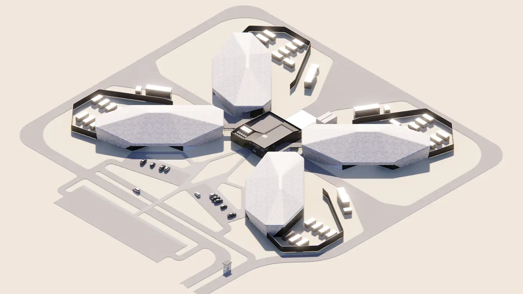
Nanotronics promises modular, shippable chip fab facilities powered by Nvidia GPUs and AI
Not to be confused for a semiconductor fab, these facilities only require two acres of land

Speaking to The Wall Street Journal, Nanotronics founder and CEO Matthew Putman hopes their CubeFab design will be seen as "a model for the way things should be produced in the future." The CubeFab model involves using modular power switch fabrication units, which come with bundled AI software and hardware to assist manufacturing and, ideally, greatly lower the barrier of entry.
Nanotronics' switch fabrication units start at 1,715 square meters. Four units with a central service cube comprise a proper CubeFab, which requires 7,510 square meters— or ten acres of land. The fabrication is for the switches used to route data center power or invert for electric vehicles, and they are considered an "ugly stepchild," according to Forrester analyst Glenn O'Donnell, cited in WSJ's original coverage.
The Nanotronics CubeFab central service cube is stated to have "some Nvidia GPUs running AI software", automating some engineering processes. The suite for the AI software costs $400,000 to $3 million based on sensor streams and data volume, according to Nanotronics.
The main manufacturing capacity per fab is found in two clean rooms, each 172 square meters, and made of materials with inherent ESD protection, like coated aluminum.
For shipping purposes, modular fab pieces can be fit on a 40-foot shipping container or flatbed truck. But even once you've paid for the fabs, regulatory issues may arise due to high power needs. Each fab is 2.7 megawatts a day, scaling to 8.7 consumption at four fabs. So, not all locations will be ideal for running these modular CubeFab setups.
So, yes, you won't be building CPUs or GPUs with these CubeFabs anytime soon. However, the big bursts of funding going into things like the CHIPS Act may still improve stateside expectations for manufacturing.
At the end of the day, this being successful could help a lot of entities who otherwise couldn't enter the semiconductor manufacturing game make their way in— and the U.S. isn't the only country set to benefit. Most of Nanotronics' current business is international, and their business model is targeted at universities and large businesses to have onsite chip manufacturing.
Get Tom's Hardware's best news and in-depth reviews, straight to your inbox.

Christopher Harper has been a successful freelance tech writer specializing in PC hardware and gaming since 2015, and ghostwrote for various B2B clients in High School before that. Outside of work, Christopher is best known to friends and rivals as an active competitive player in various eSports (particularly fighting games and arena shooters) and a purveyor of music ranging from Jimi Hendrix to Killer Mike to the Sonic Adventure 2 soundtrack.
-
Blastomonas I read a lot of articles these days about making new chips for AI and about how we need more and more, but I'm left wondering if they being used for any real purpose.Reply
Feels a little bit like the dot com boom and I'm waiting for some kind of collapse. It may simply be that my life is so far removed from Silicon valley that it seems a little ott. -
edzieba Reply
Then you didn't read the article, because this isn't about making chips for AI. The fab is for making power ICs, specifically Gallium substrate FETs.Blastomonas said:I read a lot of articles these days about making new chips for AI -
Blastomonas Reply
This is a worthwhile response, followed by another worthwhile response. Clearly the article was AI related.edzieba said:Then you didn't read the article, because this isn't about making chips for AI. The fab is for making power ICs, specifically Gallium substrate FETs. -
renz496 Reply
the article did not talk about thisBlastomonas said:I read a lot of articles these days about making new chips for AI
the article actually talking about this stuff.Blastomonas said:but I'm left wondering if they being used for any real purpose.
yes it is AI related. but you initial post talk about making new chip for AI when the actual article talk about using AI to assist chip manufacturing. even asking what's the use of AI when the article point out one it's usage.Blastomonas said:Clearly the article was AI related.