Intel Introduces World’s Largest FPGA With 43.3 Billion Transistors
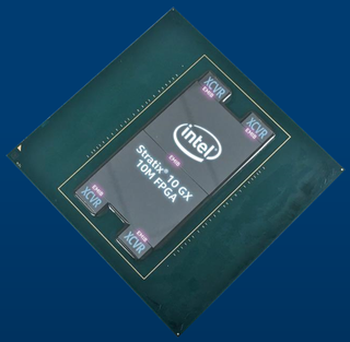
Intel today introduced the world’s highest capacity FPGA, a large chiplet package with 43.3 billion transistors. The Stratix 10 GX 10M has 10.2 million logic elements and uses EMIB to stitch two FPGA dies together along with four transceiver chiplets.

In August, Xilinx made headlines in the FPGA industry with its 16nm Virtex UltraScale+ VU19P as the word’s highest-capacity FPGA. It was its third FPGA that used an interposer to connect four dies. The VU19P had 9 million logic elements and 35 billion transistors. Other specifications included 4.5Tb/s of transceiver bandwidth and 2072 user I/O pins.
Intel is now one-upping Xilinx with the announcement of the aptly named Stratix 10 GX 10M. The 10M is composed of two large FPGA dies and four transceiver tiles. It has a total of 10.2 million logic elements and 2304 user I/O pins. This compares to the 2.75 million logic elements and 1160 I/O connections of the Stratix 10 GX 2800, Intel’s previous largest FPGA, meaning that it features nearly four times as many logic elements and twice the I/O for increased flexibility.
Further, Intel claims the 10M delivers a 40% power reduction at equivalent capacity. Intel measured this by using four Stratix 10 2800s at the same capacity and frequency as the 10M.
Intel is following a slightly different approach than Xilinx for connecting the dies. Rather than an interposer, Intel continues to use its EMIB 2.5D packaging technology that provides a high-bandwidth bridge between two adjacent dies via a relatively small piece of silicon. The EMIB data interface bus has 25,920 connections. Since each connection has a 2Gb/s throughput, this makes for an inter-die bandwidth of 6.5TB/s.


This is, in fact, the first time that Intel is using EMIB to connect two large logic dies together. Until now, Intel had limited EMIB to connect HBM to the Vega GPU in Kaby Lake-G and to connect various HBM and transceiver chiplets to the base Stratix 10 FPGA.
As part of the Stratix 10 series, the new FPGA is built on Intel’s 14nm process. Intel stated that the 10M contains 43.3 billion transistors. A rough estimate based on the provided package size yields a combined size of the two big dies of ~1400mm2 and a density of ~31MTr/mm2. This makes it the biggest silicon logic package that we are aware of. Xilinx’s 7nm Versal series currently tops out at 37 billion transistors. Nvidia's near-reticle sized (the die size limit for monolithic dies) V100 has 21.2 billion transistors in 815mm2.
Stay on the Cutting Edge
Join the experts who read Tom's Hardware for the inside track on enthusiast PC tech news — and have for over 25 years. We'll send breaking news and in-depth reviews of CPUs, GPUs, AI, maker hardware and more straight to your inbox.
Other specs appeared to be less of a focus, as its 7k 18x19 DSP multipliers and 308Mb of memory are in line with other Stratix 10 GX FPGAs. It also has four transceiver chiplets that deliver 0.84Tb/s of bandwidth.
The primary target application of the high capacity FPGA is ASIC development. Intel says that it is already shipping production silicon to customers, referring to the fast time to market it can achieve by leveraging chiplet technology. But it is unlikely that the Stratix 10 GX 10M is a last-minute reaction to Xilinx’ announcement since Intel did not already have a 14nm FPGA die with 5.1 million logic elements.
Intel started shipping Stratix 10 in volume in 2017, but the 10M is Intel’s second new FPGA in just a few months. In September, Intel introduced the Stratix 10 DX series that brought Intel’s cache coherent UPI link, PCIe 4.0, and Optane Persistent Memory to the series via a new chiplet tile.
-
JamesSneed Replymspencerl87 said:So now intel is gluing stuff together too ?
Lol they did earn that response. However this approach is pretty elegant. -
TokyoQuaSar What is your source about the number of transistor ? I can't find anything about the number of transistor in the announce by Intel.Reply -
jimmysmitty Replymspencerl87 said:So now intel is gluing stuff together too ?
Intel did it before AMD with Core 2 Quad. It was basically what AMD is doing with Zen 2 right now, 2 dies on an interposer. Hell AMD was the one back then touting a monolithic die is better than glued CPUs. This is different though as it allows for much faster communication.
JamesSneed said:Lol they did earn that response. However this approach is pretty elegant.
Extremely elegant. Its a superior system to anything they have done previously or what AMD has right now. I am excited to see what they can do with it for consumer CPUs.
Most Popular


