AMD's New Zen 3 Die Revealed In Photos
Zen 3 exposed!
Die shots of AMD's all-new 5000 series CPUs have showed up at outlet Hardwareluxx, taken by one of its community members Fritzchens Fritz, who had the courage to destroy a shiny new Ryzen 5 5600X for the sole purpose of seeing exactly what Zen 3 looks like under the hood.
Images credit: Fritzchens Fritz
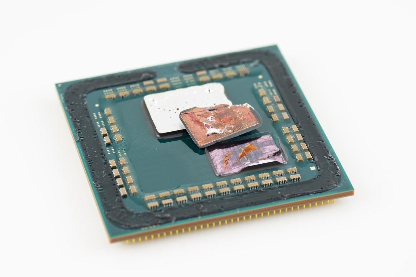
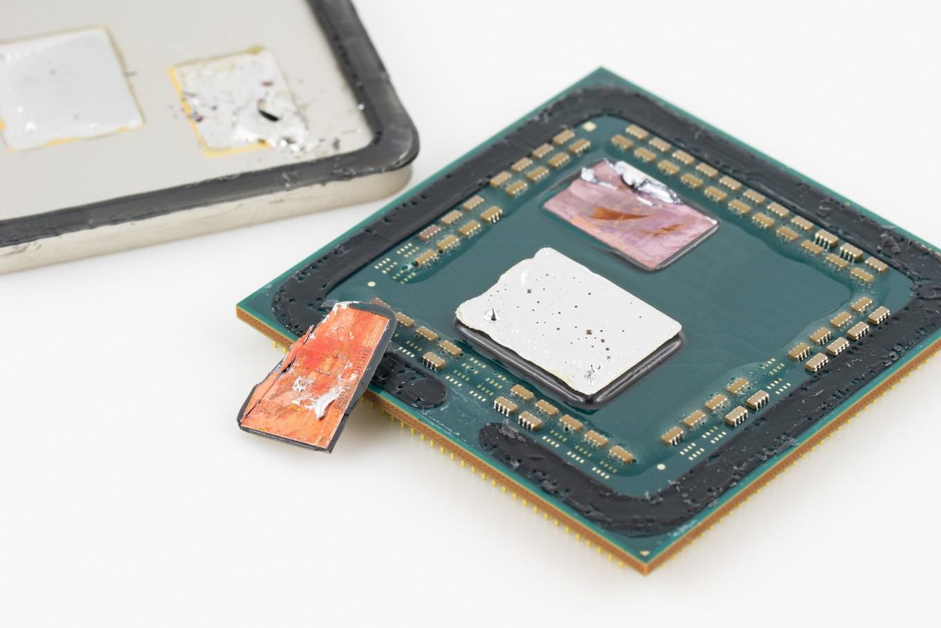
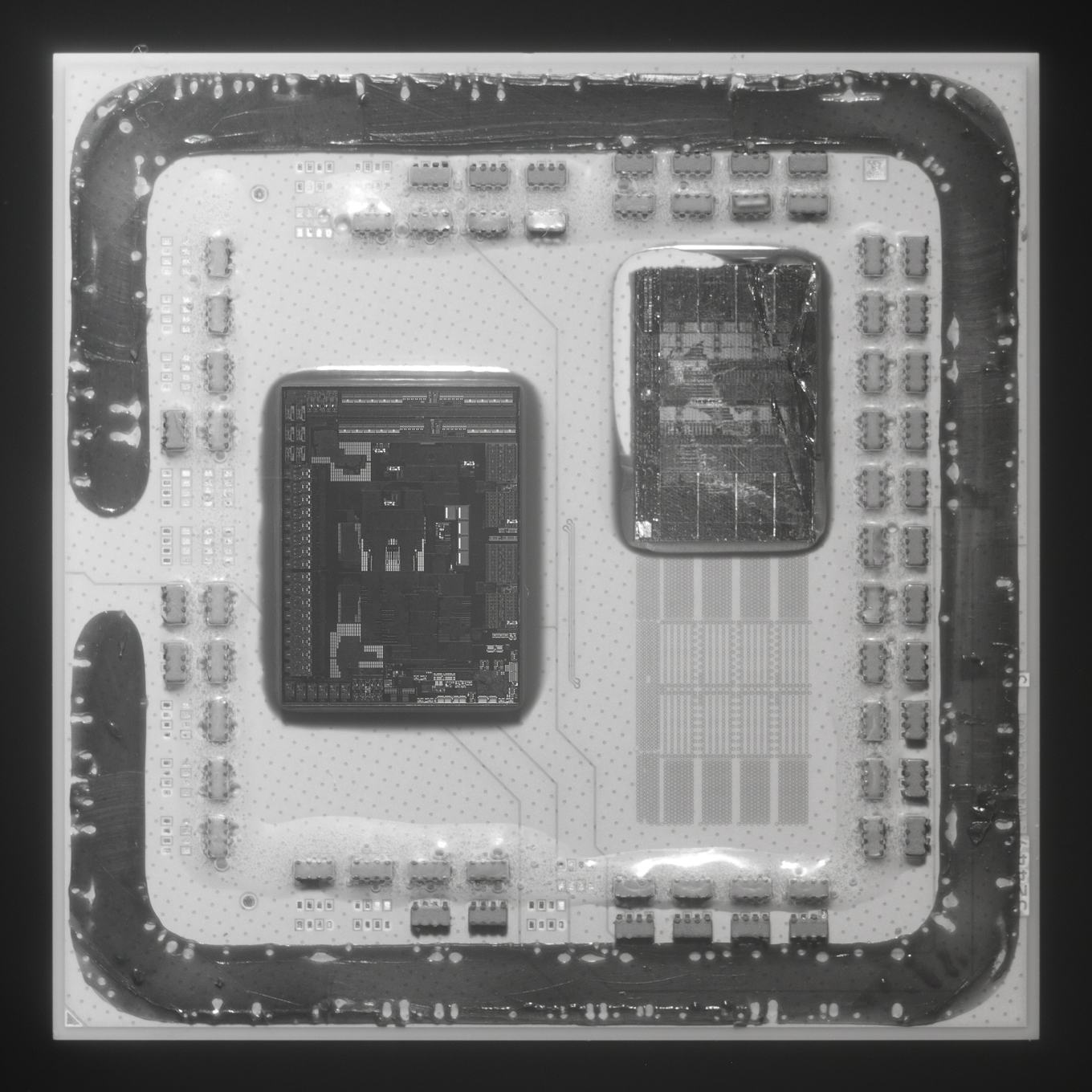
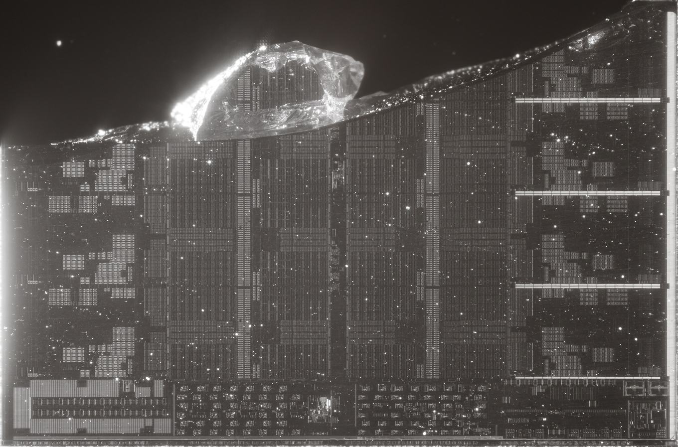
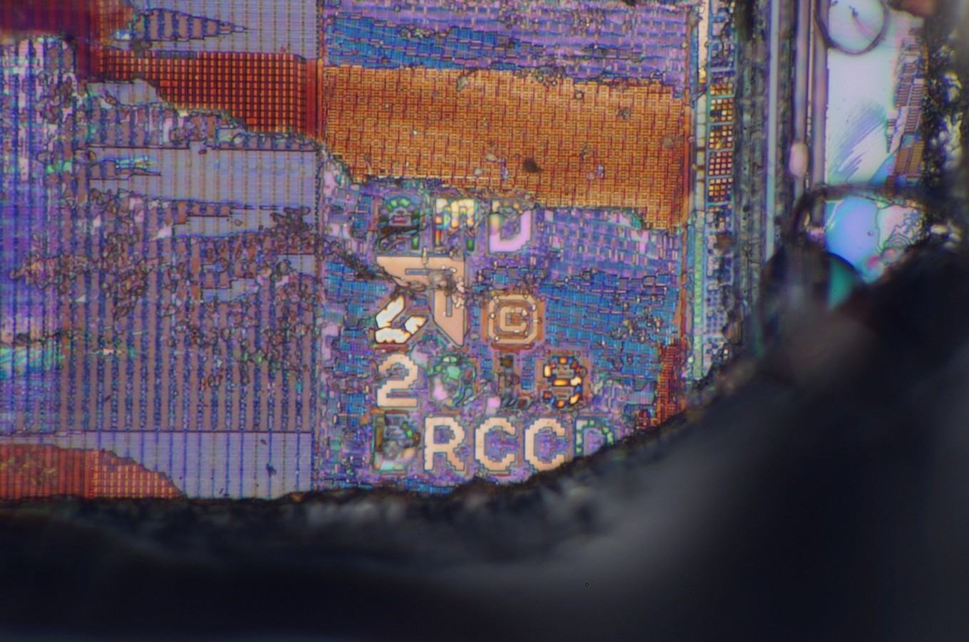
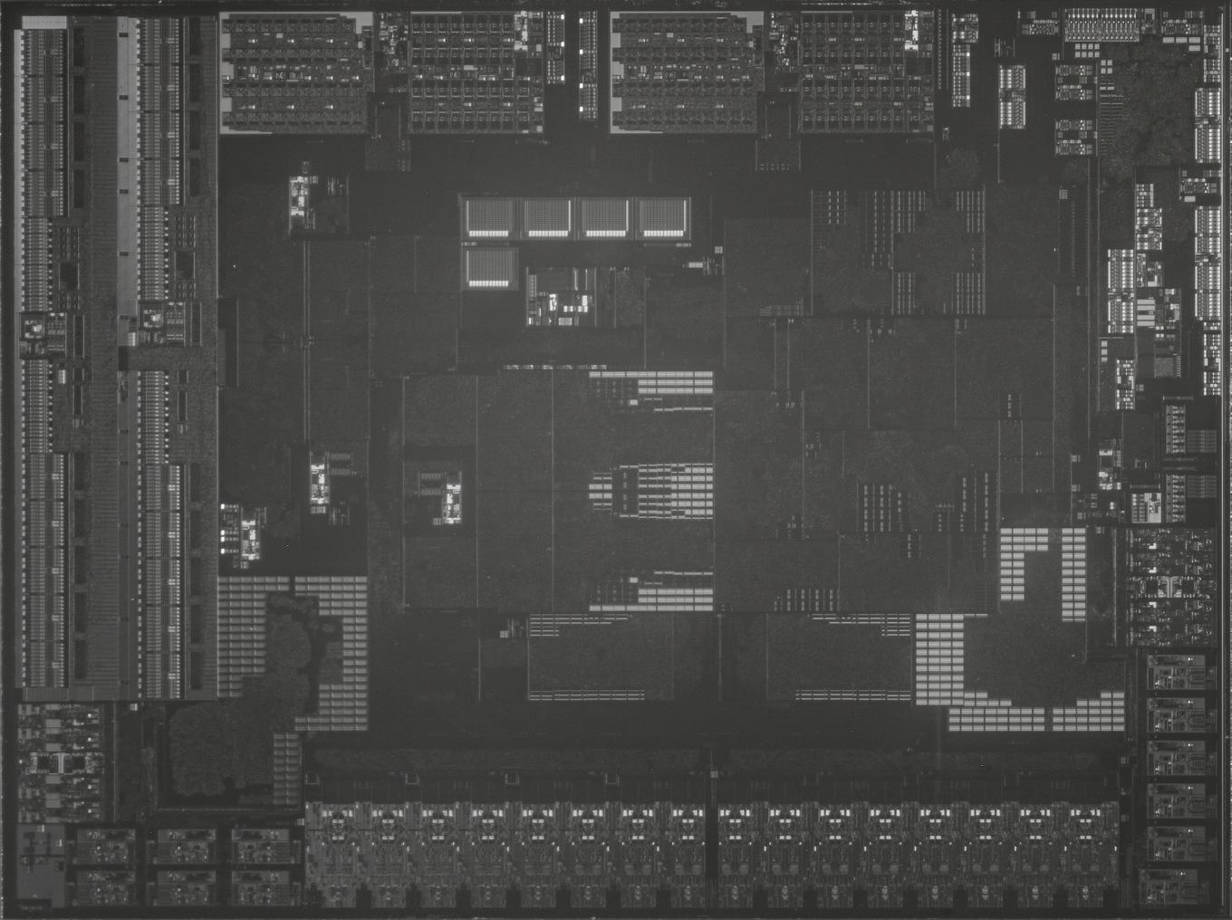
You'll notice the destruction when the enthusiast de-lidded the processor, but there are some more interesting pictures in the album. Looking at the pictures, you can see both the I/O Die (IOD) and the Core Compute Die (CCD) that houses the eight Zen 3 cores on the Ryzen 5 5600X (two of them are disabled to make a six-core chip).
We can also see the mounting pads next to the CCD for a second CCD, which would be installed for a Ryzen 9 chip. In the closeup shots, you can see some of the CPU cores themselves and the L3 cache in the middle of the CCD. Moving over to the IOD, you can see all the components that make up that unit, as well.
If you are unfamiliar with Zen 2 and Zen 3 architectures, they work on a multi-die based system. The cores and cache are housed in their own dies called CCDs, while the memory, I/O, and communication between CCDs (via the Infinity Fabric) is handled by the I/O Die. This allows AMD to use different nodes for different dies, which is more efficient for manufacturing CPUs. Specifically, the I/O die is on GlobalFoundries' older 12nm process, while the CCDs use the 7nm node from TSMC. The bigger 12nm I/O die is much cheaper to produce.
It's cool to see real shots of the new Ryzen 5000 series CCDs and I/O die, not just animated slides from AMD, even if a Ryzen 5 5600X had to be sacrificed in the process.
Get Tom's Hardware's best news and in-depth reviews, straight to your inbox.

Aaron Klotz is a contributing writer for Tom’s Hardware, covering news related to computer hardware such as CPUs, and graphics cards.
-
twotwotwo Come on, credit/link to the source (OC_Burner/Fritzchens Fritz): 1325500804434972675View: https://twitter.com/FritzchensFritz/status/1325500804434972675, 2k4xqPgView: https://www.flickr.com/photos/130561288@N04/50579552573/Reply
Not crediting people is one of the most painful things about this site. They take a bunch of lovely die shots (go back through the Flickr stream to see some). Maybe someone can hook them up with another 5600X for a try at a cleaner shot! -
rgd1101 "been taken by news outlet Hardwareluxx from one of its community members "Reply
and it link to that hardwareluxx page too -
twotwotwo Naming where you saw the pics posted isn't crediting the photographer, even if the photographer was a community member. Hardwareluxx didn't buy and decap a 5600X! This is like "crediting" Twitter or Flickr instead of the user.Reply
Flickr shows the images posted with a CC-BY license, which requires "identification of the creator(s)...(including by pseudonym if designated)." Hardwareluxx gave the pseudonym of the creator, Tom's didn't. -
DookieDraws Diffused in USAReply
Diffused in Taiwan
MADE IN CHINA
I knew AMD, like Intel, manufactures their CPUs in various fabrication plants around the world, but I never would've thought China would be involved in any of it. Very surprised, to be honest. -
cryoburner ReplySpecifically, the I/O die is on TSMC's older 12nm process, while the CCDs use the 7nm node from TSMC.
Actually, I'm pretty sure the 12nm IO chip comes from Global Foundries, not TSMC. The last I heard, they still have an agreement to get all their 12nm and larger parts from them. -
JarredWaltonGPU Reply
Just FYI, the images have proper credit listed, but our CMS apparently doesn't like to display the credit line in image galleries when all of the images aren't the same size. The third image shows the credit attribution, but none of the others do (though you can see it on the first image while the page loads). I've gone ahead and added explicit credits on all of the images, and cleaned up a bit of the text as well.twotwotwo said:Naming where you saw the pics posted isn't crediting the photographer, even if the photographer was a community member. Hardwareluxx didn't buy and decap a 5600X! This is like "crediting" Twitter or Flickr instead of the user.
Flickr shows the images posted with a CC-BY license, which requires "identification of the creator(s)...(including by pseudonym if designated)." Hardwareluxx gave the pseudonym of the creator, Tom's didn't. -
hotaru.hino Reply
https://www.tsmc.com/english/aboutTSMC/TSMC_FabsDookieDraws said:Diffused in USA
Diffused in Taiwan
MADE IN CHINA
I knew AMD, like Intel, manufactures their CPUs in various fabrication plants around the world, but I never would've thought China would be involved in any of it. Very surprised, to be honest.
TSMC has a couple of fabs in mainland China. Though the "made in" part may just be the final package assembly. -
escksu ReplyDookieDraws said:Diffused in USA
Diffused in Taiwan
MADE IN CHINA
I knew AMD, like Intel, manufactures their CPUs in various fabrication plants around the world, but I never would've thought China would be involved in any of it. Very surprised, to be honest.
Wow you sure?? Both companies have their CPU plants in China for a long long time already......But its not fab. Its testing and assembly. -
escksu Replyhotaru.hino said:https://www.tsmc.com/english/aboutTSMC/TSMC_Fabs
TSMC has a couple of fabs in mainland China. Though the "made in" part may just be the final package assembly.
The 7nm chipsets are by TSMC in Taiwan, the IO die is 14nm by glofo (itself a spinoff from AMD). The dies are assembled and tested in China.