The Tech Behind Apple's M1 UltraFusion Chip Interconnect
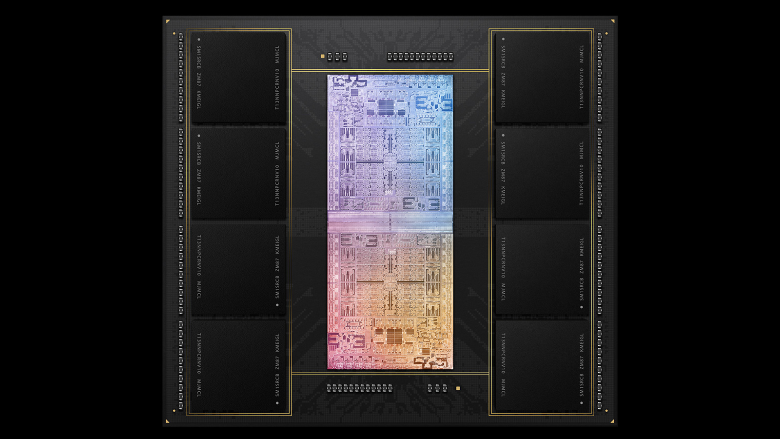
TSMC's CoWoS-S in action
Building high-performance microprocessors is getting trickier and more expensive these days, which is why developers have to opt for sophisticated packaging technologies with designs aimed at performance-hungry applications. Apple admits that to make its M1 Ultra processor it had to fuse two M1 Max system-on-chips together, but what it didn't say is that it had to use one of TSMC's most advanced packaging technologies to build the M1 Ultra.
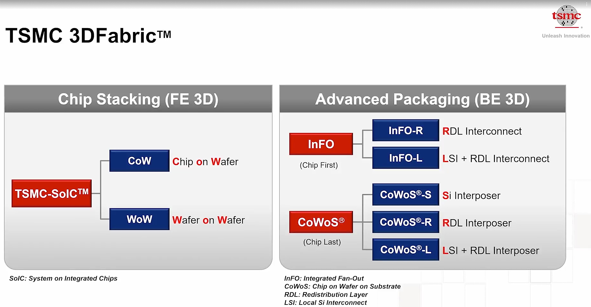
Fortunately, unofficial sources are less secretive than Apple and were able to unearth additional details about Apple's UltraFusion interprocessor interconnection that offers bandwidth of 2.5 TB/s. DigiTimes reports that Apple's M1 Ultra processor* used TSMC's CoWoS-S (chip-on-wafer-on-substrate with silicon interposer) 2.5D interposer-based packaging process to build the M1 Ultra. Similar technologies are used by companies like AMD, Nvidia, and Fujitsu to build their high-performance processors for datacenters and high-performance computing (HPC).
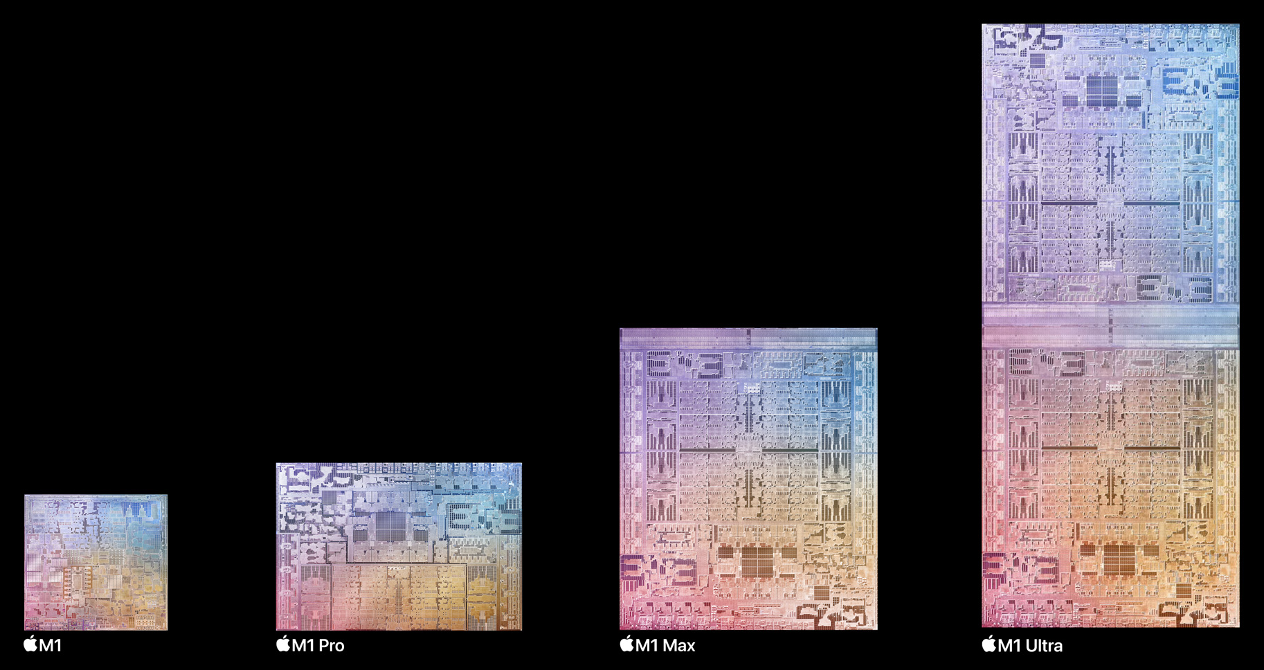
Apple's M1 Ultra is certainly a formidable design. Each M1 Max SoC feature a die size of 432 mm2, so the interposer that the M1 Ultra uses must be over 860 mm2. That's rather massive but not unheard of. AMD and Nvidia use even bigger interposers with their compute GPUs featuring high-bandwidth memory.
* - We don't know exactly what to call the M1 Ultra. Technically, this is a system-on-chip-in-package, or SoCiP, but that can be a bit of a mouthful, so we'll just call it a "processor" for now.
But TSMC's CoWoS-S is not the only option that the world's largest contract maker of semiconductor has for bandwidth-hungry applications. Some experts have speculated that Apple could opt for TSMC's InFO_LSI technology for the ultra-high bandwidth chiplet integration. Unlike CoWoS-S, InFO_LSI uses localized silicon interconnects instead of large and expensive interposers. Intel's embedded die interconnect bridge (EMIB) uses the same concept.
Keeping in mind that Apple demonstrated an M1 Max die shot with a massive I/O pad that resembles a local interconnect designed to connect to an intermediary chip, it's no surprise that many people thought that Apple used InFO_LSI.
But there's a reason Apple may have stuck to the potentially more expensive CoWoS-S. TSMC's InFO_LSI was formally introduced in August 2020 and was meant to complete qualification in Q1 2021. Meanwhile, Apple's M1 Max was set to enter volume production in Q2 or Q3 2021, so Apple may simply not have had enough time to implement InFO_LSI. That or it decided not to take a risk and stick to a well-known technology that is widely used by various companies.
Another item that DigiTimes discloses is that Unimicron Technology is now the only supplier of ABF (Ajinomoto build-up film) substrates to Apple, as it is the only company that can deliver the quality and quantity that Apple needs. Anyway, while we now know what packaging technology Apple used to enable its UltraFusion interconnect, we still have no idea about its clocks, bus width, power, etc., so stay tuned.
Get Tom's Hardware's best news and in-depth reviews, straight to your inbox.

Anton Shilov is a contributing writer at Tom’s Hardware. Over the past couple of decades, he has covered everything from CPUs and GPUs to supercomputers and from modern process technologies and latest fab tools to high-tech industry trends.


