Just weeks after PCI SIG released the final draft of PCIe 6.0 specifications, Cadence introduced one of the industry's first silicon-proven IP packages that enable chip developers to implement PCIe 6.0 support into their designs and test it. The IP is available now and will enable early adopters to add support for PCIe 6.0 to chips due in 2022 - 2023.
"Early adopters have already started exploring with the new PCIe6 specification, and we are looking forward to seeing them achieve positive results with TSMC and Cadence technologies," said Sanjive Agarwala, corporate vice president and general manager of the IP Group at Cadence in a statement.

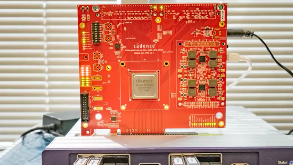
Along with the IP package, Cadence also offers a PCIe 6.0 test chip implemented using N5 and meant to test signal integrity and performance of PCIe 6.0 implementations at all data rates.
The chip contains a PAM4/NRZ dual-mode transmitter that is guaranteed to provide optimal signal integrity, symmetry and linearity with low jitter as well as a receiver that can withstand harsh signal impairments and channel loss in excess of 35dB at 64GT/s to provide sophisticated data recovery capabilities. Since with PCIe 6.0 chip developers will be dealing with data transfers at up to 64 GT/s over relatively long traces (for comparison, DDR5 memory currently has a transfer rate of 4.8 GT/s – 7.0 GT/s), ensuring signal integrity and supporting sophisticated data recovery mechanisms becomes a must.
"We have been deploying PAM4-based IP since 2019 when we introduced our first-generation 112G-LR SerDes IP, and our vast expertise in PAM4 technology plus our strong collaboration with TSMC provides a robust foundation for success with our PCIe6 products," said Agarwala.
