China's Blacklisted YMTC Ships World-Leading 232-Layer 3D QLC NAND
TechInsights finds bleeding-edge 3D QLC NAND-based SSD.

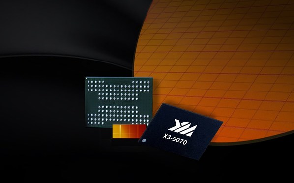
China-based Yangtze Memory Technologies (YMTC) has quietly started shipments of 3D QLC NAND memory with 232 active layers, TechInsights has discovered. The new 3D NAND memory devices boast the industry's highest recording density of as well as extreme performance due to Xtacking 3.0 architecture.
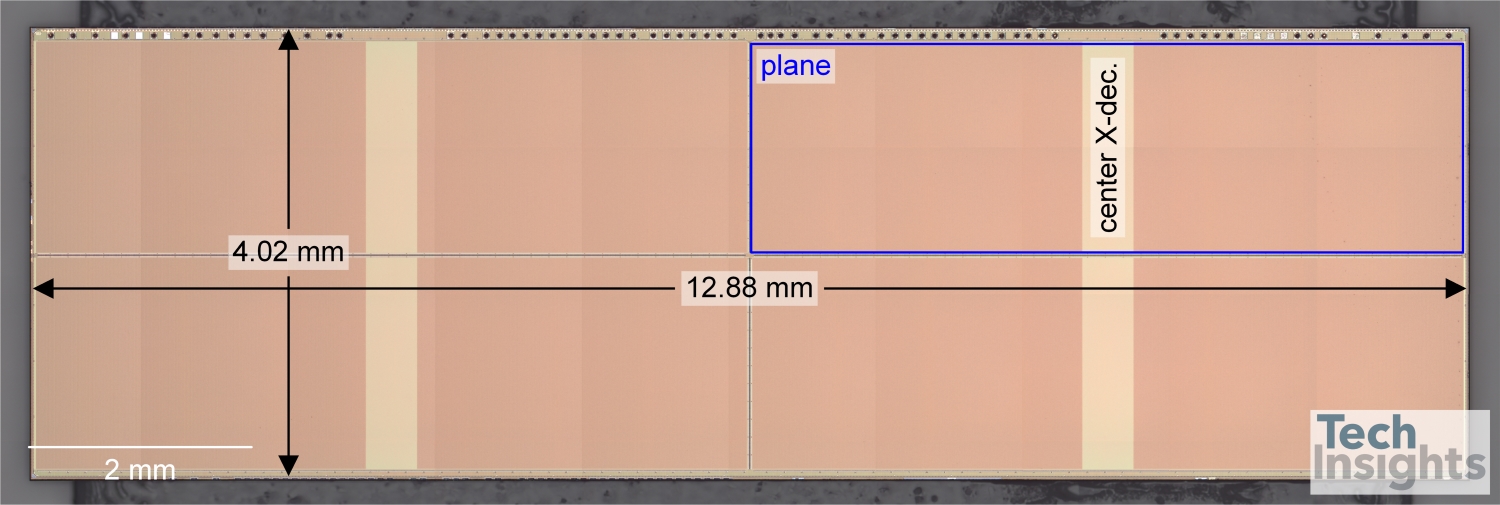
YMTC's 1Tb 3D QLC NAND device has a recording density of 19.8 Gbit/mm2, which is the world's highest density for a commercial IC. In fact, even a 232-layer 3D TLC NAND chip from YMTC boasts a recording density of 15.47 Gbit/mm2, which is higher than competing offerings that are in mass production.
There is a substantial difference between the 3D QLC and 3D TLC NAND devices from YMTC: The former features a quad-plane design to optimize die size, whereas the latter features a six-plane design to maximize performance. Meanwhile, both ICs use Xtacking 3.0 architecture as well as a 2400 MT/s data transfer rate, so both could be used for the best SSDs featuring a PCIe 4.0 or PCIe 5.0 interface.
One interesting thing to note is that analysts from TechInsights discovered YMTC's 1Tb 3D QLC NAND devices in a ZhiTai Ti600 1TB solid state drive, which was quietly launched in July, 2023, and has been on the market since then. YMTC has been producing this memory for over a quarter now. Yet, it is unclear whether it can produce such memory in substantial quantities.
Producing such memory devices is a major achievement for YMTC, which is blacklisted by the U.S. government and cannot obtain leading-edge tools from American companies. Meanwhile, the company has managed to achieve the highest recording density with its 3D TLC NAND with 232 active layers, surpassing its rivalsprimarily due to its Xtacking 3.0 architecture that relies on hybrid bonding.
Get Tom's Hardware's best news and in-depth reviews, straight to your inbox.

Anton Shilov is a contributing writer at Tom’s Hardware. Over the past couple of decades, he has covered everything from CPUs and GPUs to supercomputers and from modern process technologies and latest fab tools to high-tech industry trends.
-
ivan_vy in the end sanctions didn't stop the dragon. Government funding R&D and a market too big make economy of scale feasible. They might be behind now but in the long term their products will be good enough and better in some instances. Outsourcing And Offshoring profits came with a -not so hidden- price.Reply -
ThomasKinsley It's worth reading how committed Yangtze Memory Technologies was to making this happen. Based in Wuhan, Yangtze Memory Technologies saw a flurry of activity as trains continued to ferry experts back and forth to work during the height of the 2020 pandemic even as the rest of China was under lockdown.Reply
https://web.archive.org/web/20200705020643/https://asia.nikkei.com/Spotlight/The-Big-Story/How-China-s-chip-industry-defied-the-coronavirus-lockdown -
The Historical Fidelity This is to be expected since YMTE had access to purchase the appropriate tooling to manufacture 232 layer NAND until recently. The real benchmark for the affects of sanctions will be YMTE’s ability to stay competitive with higher layer counts in the future without access to the future western tooling.Reply -
George³ May I assume that the total number of computer professionals in China is greater than in the US, and that a greater percentage of them are engaged in progressive work? While in the US, a large percentage work in the entertainment industry and the advertising sector.Reply -
anonymousdude ReplyThe Historical Fidelity said:This is to be expected since YMTE had access to purchase the appropriate tooling to manufacture 232 layer NAND until recently. The real benchmark for the affects of sanctions will be YMTE’s ability to stay competitive with higher layer counts in the future without access to the future western tooling.
Exactly, YMTC has all the machinery they needed to create this. It's not like it's some massive surprise or anything. The sanctions were never going to prevent any near term product development. The sanctions are to curtail future development. Give it a couple of years and let's see if YMTC can produce 300, 400, 500+ layer NAND. That's when you know if the sanctions are working.
Also, outside of Micron, every other major player in the NAND space effectively delayed their 200+ layer NAND products due to the current oversupply. Funny what happens when you commoditize something and spot pricing tanks for the commodity. -
George³ Even the most advanced NAND flash today is made with mature lithographic nodes that are several generations ahead of those affected by the sanctions. Maybe "5"nm will meet nand flash only after 10 years. Number of layers isn't depending of nanometers and not related to existing sanctions.Reply -
The Historical Fidelity Reply
You may not, thank youGeorge³ said:May I assume that the total number of computer professionals in China is greater than in the US, and that a greater percentage of them are engaged in progressive work? While in the US, a large percentage work in the entertainment industry and the advertising sector. -
The Historical Fidelity Reply
YMTC cannot requisition new high aspect ratio etching instruments or metrology tools from the west, this will greatly affect their ability to increase layer count as the through stack bore hole becomes deeper and deeper for example.George³ said:Even the most advanced NAND flash today is made with mature lithographic nodes that are several generations ahead of those affected by the sanctions. Maybe "5"nm will meet nand flash only after 10 years. Number of layers isn't depending of nanometers and not related to existing sanctions. -
George³ Reply
In article didn't mentioned etching. Where your knowledge about this come from? And where is determined in sanctions documents?The Historical Fidelity said:YMTC cannot requisition new high aspect ratio etching instruments from the west, this will greatly affect their ability to increase layer count as the through stack bore hole becomes deeper and deeper. -
The Historical Fidelity Reply
That’s because Tom’s Hardware is not a semiconductor engineering journal.George³ said:In article didn't mentioned etching. Where your knowledge about this come from? And where is determined in sanctions documents?
It’s known industry knowledge.
