IBM Could Use DNA to Make Next-Gen Chips
DNA to make chips. Sounds like sci-fi, but it's not.
Get Tom's Hardware's best news and in-depth reviews, straight to your inbox.
You are now subscribed
Your newsletter sign-up was successful
Chip makers are always looking for the next big breakthrough in making smaller, faster, more energy efficient computer chips. IBM, always pushing its research and development teams, claims to have found a potential new chip making method using nanotechnology.
In conjunction with the California Institute of Technology collaborator Paul W.K. Rothemund, IBM Research has published its findings on an advancement in combining lithographic patterning with self assembly – a method to arrange DNA origami structures on surfaces compatible with today’s semiconductor manufacturing equipment.
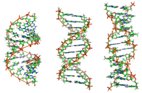
Current manufacturing techniques focus on making feature sizes smaller than 22-nm, and IBM's approach of using DNA molecules as scaffolding could be the way there. IBM explained that millions of carbon nanotubes could be deposited and self-assembled into precise patterns by sticking to the DNA molecules. Specially positioned DNA nanostructures can serve as scaffolds, or miniature circuit boards, for the precise assembly of components – such as carbon nanotubes, nanowires and nanoparticles – at dimensions significantly smaller than possible with conventional semiconductor fabrication techniques.
The paper on this work, “Placement and orientation of DNA nanostructures on lithographically patterned surfaces,” by scientists at IBM Research and the California Institute of Technology, will be published in the September issue of Nature Nanotechnology. Those with an online account may access it now here.
Get Tom's Hardware's best news and in-depth reviews, straight to your inbox.
-
Burodsx I've read about this a few months ago. The idea is to make DNA attach to the material, then remove the DNA once it is formed. The process is supposed to be cost effective and better all-around. The article mentioned manufacturing to approximately the 7-9nm level. Hopefully they can make this work sooner rather than later.*crosses fingers*Reply -
paranoidmage The hydrogen bonds holding two strands of DNA together break at low temperatures, around 55 degrees Celsius. I don't know how strong the individual strands are, but I wouldn't want my CPU to denature when I run Prime95.Reply -
megabuster paranoidmageThe hydrogen bonds holding two strands of DNA together break at low temperatures, around 55 degrees Celsius. I don't know how strong the individual strands are, but I wouldn't want my CPU to denature when I run Prime95.DNA is only used to build the processor; they are not building an organic CPU.Reply -
Burodsx The DNA is removed after forming the desired product. Hence think of the DNA as a mold.Reply -
mlopinto2k1 If they used Chuck Norris' DNA the chip would remove the nanotubes and just use the DNA.Reply -
teeth_03 mlopinto2k1If they used Chuck Norris' DNA the chip would remove the nanotubes and just use the DNA.Reply
Chuck Norris's DNA could max out Crysis...Twice... -
rambo117 megabusterDNA is only used to build the processor; they are not building an organic CPU.that would be nasty lol.Reply

