Japanese Scientists Create RAM Storage Based on Light
NTT Labs has succeeded in building a prototype of what the company calls optical random access memory, or short o-RAM.
The idea is to remove the bottleneck between fiber optics and electronic circuits and create a light-speed version of today's DRAM architecture for high-speed data center applications.
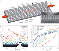
According to a research paper published in Nature Photonics, the prototype has a capacity of 4 bits and transfers data at 40 Gbps. It features extremely low power consumption at just 30 nW. While it is far from a commercial product, the researchers believe that it is a foundation for the development of far more capable o-RAM devices with a storage capacity in the range of Kb or Mb. The NTT researchers believe that a 100 Kb o-Ram for all optical network routers device could be built by 2020. A 1 Mb o-RAM chip could be available by 2025.
Each memory cell of the new technology is a nano-photonic crystal that ismade from indium phosphide that integrates a small strip of gallium arsenide phosphide. The flow of laser light is controlled via tiny holes on the outer portion of the cell, while a path in the middle of the crystal was created to allow light to enter and exit the device. Each cell can represent the values 1 or 0 by either transmitting light or blocking it by changing the refraction index of the material. Once a value is set, background light sourced from a laser maintains the refraction index.
Article continues belowThe approach apparently enabled the scientists to store data for up to 10 seconds, which is up from 250 nanoseconds in previous similar devices.
Get Tom's Hardware's best news and in-depth reviews, straight to your inbox.

Douglas Perry was a freelance writer for Tom's Hardware covering semiconductors, storage technology, quantum computing, and processor power delivery. He has authored several books and is currently an editor for The Oregonian/OregonLive.
-
victorious 3930k By then 1TB+ RAM will be standard. Who cares if it's deadly fast if it can't run their apps!Reply -
yumri this is a good advancement but needs to be alot bigger at least 64K - 128MB for a router in a optical network. I am glad to see this is being done and really hope the bandwidth gets bigger and the time which data can be stored gets longer as 10 seconds would mean alot of ARP calls throughout the network which were not there with electronic RAM and thus more overhead even though it is faster.Reply -
yumri also @victorous 3930K this is NOT for your PC this is for network equipment which typically use high speed 64K chips at most they are 128K chips so yeah we might have a 1TB hard drive but that would be total overkill for a piece of equipment in the target market for the light RAM.Reply
Also Light based computers failed in the consumer market because they were not cheap enough and were not that practical for the consumer. -
upgrade_1977 Always wondered where do they come up with the dates? With the current advancement in electronics i'm sure someone will come up with a 1gb ver. in a few years..Reply -
A Bad Day victorious 3930kBy then 1TB+ RAM will be standard. Who cares if it's deadly fast if it can't run their apps!Reply
Look pal, there's a reason why DRAM is never used as a cache for processors, or why processors even have cache. DRAM's latency is way too high for such high CPU performance, especially if you have the DRAM located a few centimeters away from the CPU.
I don't care about your hexacore 6 GHz processor if it doesn't have enough cache or none at all, because it's going to spend almost all of its cycles on waiting for the DRAM to respond and end up being a really hot .1 GHz processor.
