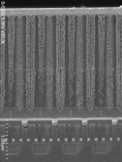
Elpida shrinks production process for DDR2 SDRAM to 90nm
Get Tom's Hardware's best news and in-depth reviews, straight to your inbox.
You are now subscribed
Your newsletter sign-up was successful
Tokyo - Elpida announced that it will start to manufacture DDR2 memory in 90nm, down from the current 100 nm generation. The transition will allow the manufacturer to yield more chips per wafer and cut production cost.
According to the firm, the development of the new silicon wafer production process has been completed and will be applied to mass production early next year. The technology will first be used for 512 Mbit and 1 Gbit DDR2 SDRAM products. The company believes that moving from 100nm to 90 nm will increase productivity by about 20 percent.
Elpida is using the same 248 nm-wavelength KrF optical lithography that is used for current mass production of 100 nm devices in its new 90 nm lines. In combination with the use of Optical Proximity Correction (OPC) the new process refines and reduces the geometric size of the memory cell and its peripherals by 90% "while maintaining high production yields", Elpida said. Manufacturers typically do not reveal yield rates of their chips.
Elpida is second to announce 90 nm memory. Samsung announced back in August that it would move to 90 nm DDR2 memory. Samsung also recently announced that the company intends to increase its market share to about 75 percent, mainly by lowering prices of its products.
Get Tom's Hardware's best news and in-depth reviews, straight to your inbox.

Wolfgang Gruener is an experienced professional in digital strategy and content, specializing in web strategy, content architecture, user experience, and applying AI in content operations within the insurtech industry. His previous roles include Director, Digital Strategy and Content Experience at American Eagle, Managing Editor at TG Daily, and contributing to publications like Tom's Guide and Tom's Hardware.
