Imec Fabricates Beyond-Silicon MoS2 2D Transistors
Who needs silicon, anyway?

Get Tom's Hardware's best news and in-depth reviews, straight to your inbox.
You are now subscribed
Your newsletter sign-up was successful
Imec has fabricated nanoscale transistors with the 2D material MoS2. They confirmed theoretical findings and showed promising performance. Such transistors have the potential to replace today’s FinFETs and continue transistor scaling.
MoS2, Molybdenum disulfide in full, is one of many two dimensional (2D) semiconductor materials. It has a thickness of just three 0.6nm atomic monolayers. At IEEE’s annual International Electronic Devices Meeting (IEDM), Belgian microelectronics research organization Imec has presented an in-depth study of highly scaled MoS2-based transistors.
According to Imec, the findings confirm the potential of 2D materials for ultra-scaled transistors for both high-performance logic and memory, as theoretical studies had shown that they show little short-channel effects compared to silicon channel transistors. The fabricated devices performed largely in accordance with TCAD simulations. They are not yet on the level of modern silicon devices, but Imec says they see a path for further improvements that includes reducing defects, using two gates per transistor and further reducing the HfO2 oxide thickness.
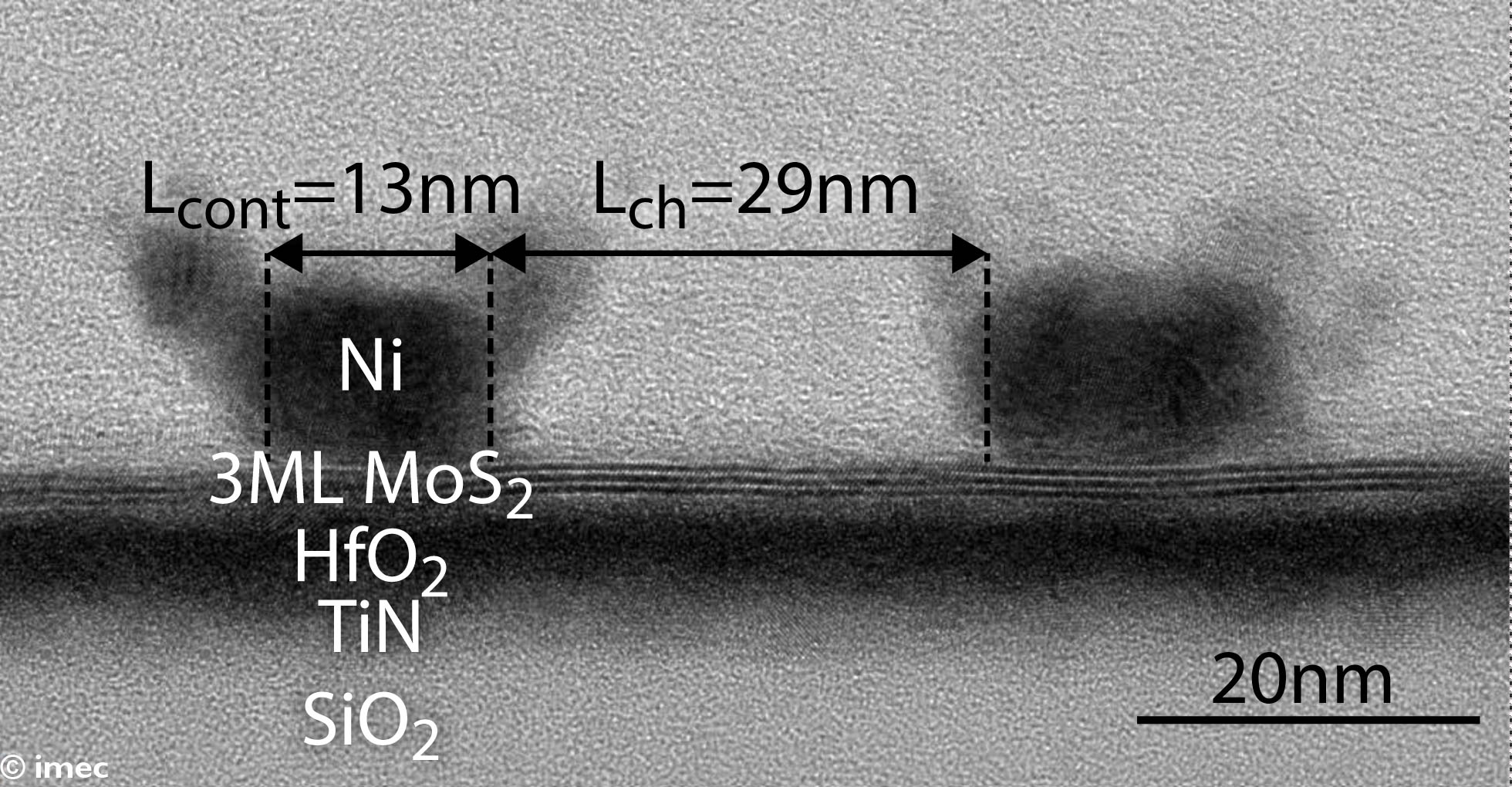
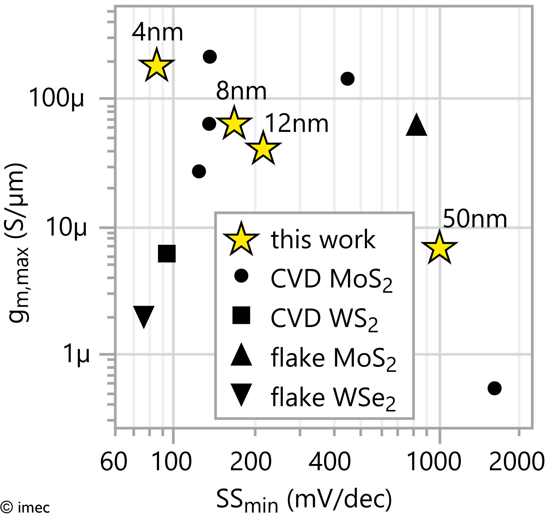
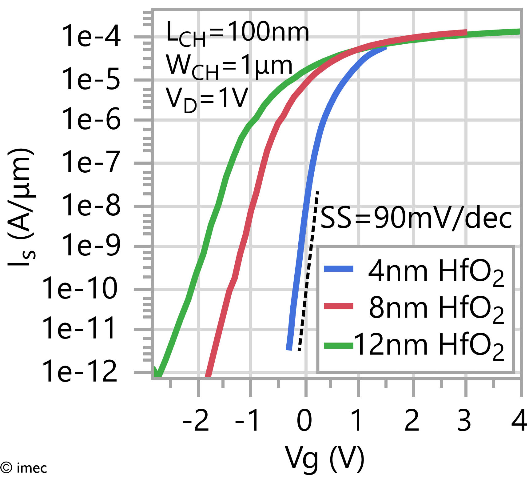
The devices that Imec fabricated had a channel length of 30nm. The contact pitch was reported as being smaller than 50nm, and the contacts themselves had a length of 13nm. For comparison, Intel’s 10nm process has a channel length of 18nm and a contacted gate pitch of 54nm. The highest-performing devices had 4nm HfO2 high-k dielectrics; Imec also tested 8nm, 12nm and 50nm SiO2 devices. The sub-threshold slope was as low as 80mV/dec, similar to early FinFETs.
Although still an order of magnitude away from Si transistors, we have brought our MOSFET devices into a realm where they show promising performance for future logic and memory applications. To bridge this order of magnitude, we have identified a path of systematic improvements such as a further reduction of the gate oxide thickness, the implementation of a double-gated architecture, and further reduction of channel and interface defects. We are transferring this insight to our 300mm-wafer platform for transistors with 2D materials, which was announced at last year’s IEDM.
Iuliana Radu, Imec Director


Imec’s role as research institution for process technology is to explore the limits of semiconductor device scaling through new and enhanced technologies. Imec CEO Luc Van den Hove explained how its MoS2 research fits in that model: “Our partners expect us to lead the way and to support them in realizing their roadmaps by demonstrating the potential of innovative concepts and novel materials. This is why I am so thrilled we have demonstrated excellent performance in ultra-scaled devices with 2D materials, and a credible path to further improvements aiming at mass production in industrial 300mm fabs.”
2D materials are just one option among many so-called beyond-silicon or beyond-CMOS devices that are in various stages of research. The front-runner is the gate-all-around (GAA) FET, also called nanosheet or nanowire transistors. As an evolution of the 3D-channel FinFET transistor, Samsung has announced that it will adopt it at its 3nm node. TSMC is expected to introduce it in its 2nm process, and Intel in its 5nm process.
The research is one of 24 papers (PDF) Imec has submitted for IEDM 2019. Other work presented at the IEDM 2019 conference includes a 2MB MRAM array for L4 caches by Intel.
Get Tom's Hardware's best news and in-depth reviews, straight to your inbox.