Micron Announces 16nm TLC NAND
Micron announced its new 16nm TLC NAND at Computex 2015. The continuing expansion of flash-based products for mobile devices, PCs, and data centers requires more capacity every year. The cost of NAND-based products continues to fall through a combination of shrinking the lithography and increasing production capabilities. To increase manufacturing output, the vendors also have the capability of packing more bits into each NAND cell, which increases the storage capacity within the same space.
At a high level, NAND is divided into three classes: SLC, MLC and TLC. SLC stores one bit-per-cell, MLC stores two bits-per-cell and TLC provides the ultimate in density with 3 bits-per-cell. In a perfect world the NAND vendors could just continue cramming more bits into each cell, but increasing the number of bits reduces performance and endurance, which means that the NAND will not last as long.
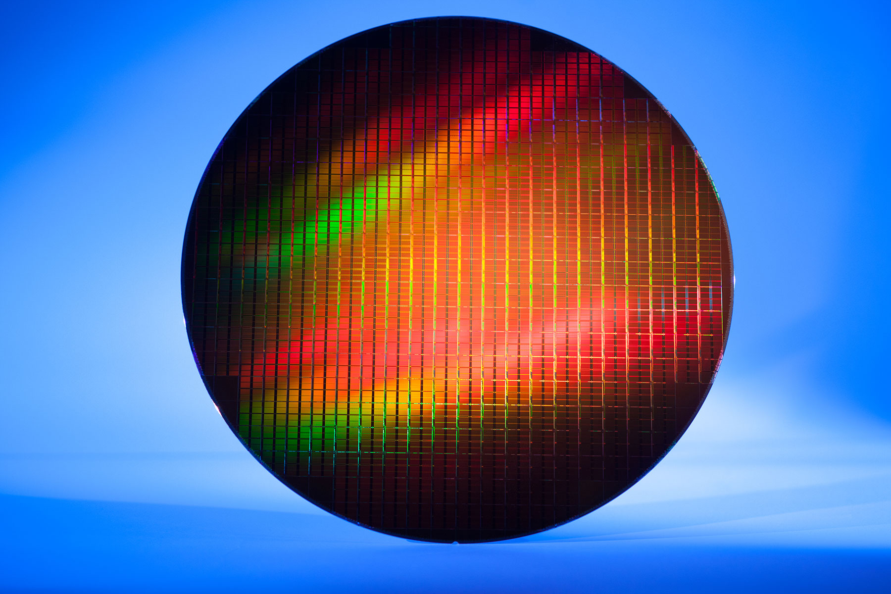
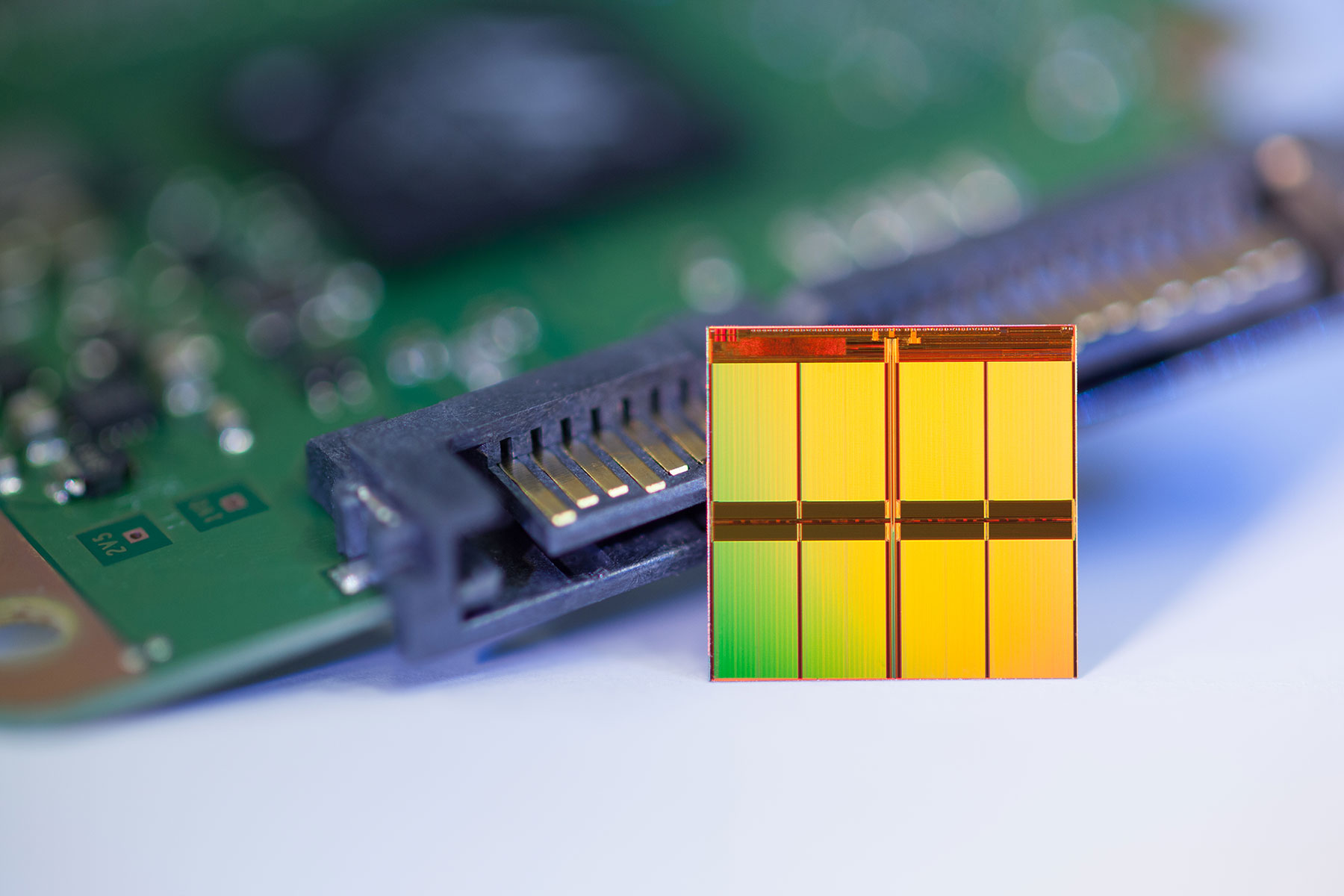
What are the benefits of packing in more bits? Increasing the density reduces the cost, which means more cheap SSDs for our devices. The addition of three cells in Micron's 16nm NAND enables a 28 percent increase in density. A single Micron 16nm TLC die can store up to 16 GB, but each die is merely a small portion of an overall wafer. One 300 mm wafer, pictured above, can create nearly 6 TB of storage. Micron's 16nm TLC product still utilizes the standard 2D design (planar) that has been used for years. Intel/Micron 3D NAND products are also coming to market, but Micron will continue to sell 16nm, largely because it will be a more profitable product until 3D NAND process matures.
Article continues below"Our new TLC NAND technology meets the ever-rising demand for reliable high-capacity storage," said Kevin Kilbuck, director of NAND planning at Micron. "We see 16nm TLC as an excellent solution for 2015 consumer applications as we drive toward 3D NAND TLC production in 2016."
TLC NAND wasn't strong enough to handle the demands of most devices even a few short years ago, but through the benefits of enhanced NAND management and clever engineering, it has become the mainstream NAND of choice. In fact, TLC is projected to constitute almost half of the NAND shipped worldwide in 2015, and by 2016 the analyst crowd expects more TLC NAND to be employed than any other type.
Samsung began shipping TLC-based products several years ago, while other vendors have continued to utilize MLC. Because TLC has reduced endurance, and thus potential reliability concerns, Micron indicates the company waited until the process and design was mature enough to ship a viable product and maintain profitability.
The Toshiba/SanDisk joint venture is also moving forward with 15nm TLC, with several finished products on display here at Computex. Micron 16nm is in production and is already sampling to its partners, and SSD controller manufacturer SMI also announced it will support the new product. We expect to see several new prototypes with 16nm TLC around the Flash Memory Summit time frame in August, and Micron indicates that end products (i.e. SSDs) will work their way to the market this Fall.
Get Tom's Hardware's best news and in-depth reviews, straight to your inbox.
Paul Alcorn is a Contributing Editor for Tom's Hardware, covering Storage. Follow him on Twitter and Google+.

Paul Alcorn is the Editor-in-Chief for Tom's Hardware US. He also writes news and reviews on CPUs, storage, and enterprise hardware.
-
razor512 So now you can have the joy of sending your SSD in for an RMA each time you save a text document onto it.Reply -
LordConrad Considering the problems Samsung ran into with the 840 EVO, I think 1x nm TLC NAND is just plain stupid.Reply -
ammaross ReplyConsidering the problems Samsung ran into with the 840 EVO, I think 1x nm TLC NAND is just plain stupid.
Good thing their 3D NAND is 42nm then. -
LordConrad Reply
Samsung did good with their 3D V-NAND. Who knows what lithography Micron and Toshiba will use for their 3D NAND, but 1x nm TLC 2D NAND is asking for trouble.15989292 said:Considering the problems Samsung ran into with the 840 EVO, I think 1x nm TLC NAND is just plain stupid.
Good thing their 3D NAND is 42nm then.
-
hannibal You can expect all market micros to have those, as well as many laptops and handheld devices... We need better information, what is inside of those pre equipped devices!Reply -
nottheking I'm still not convinced of the viability of bleeding/cutting-edge TLC NAND in SSDs; the 840 EVO definitely put a spotlight on it, though the problem really applies to more than just that. (I feel the 840 EVO just came to the forefront due to being the darling of enthusiasts upon release, hence more exposure when the problems started cropping up)Reply
Still, price will tend to win out just about every time: it's why, for instance, dangerously bad power supplies still flood the market: not enough people are aware of the dangers of their terrible capacitors and how they're going to blow in a year or two, they just know that they can get the "500w" unit their new video card demands for only $30.
For such a huge portion of the market, no other considerations are even noticed beyond simply the "price per gigabyte" number; and when it comes to that, 1x nm TLC NAND cannot really be beaten. -
RamCity From a retailers perspective, Microns investment in TLC makes sense. We have very, very few returns on 840 Evos which to me says the vast majority of consumers are happy with TLC. And it's the vast majority that Crucial are going after here, as well as partnerships with other niche vendors like Transcend who want access to low cost flash.Reply

