Nvidia Tackles Chipmaking Process, Claims 40X Speed Up with cuLitho

Mask

Intel Mask - Illustrative purposes only. (Image credit: Intel)

At GTC 2023, Nvidia announced its new cuLitho software library for speeding up a critical bottleneck in the semiconductor manufacturing workflow. The new library speeds computational lithography, a technique used to create photomasks for chip production. Nvidia claims its new approach enables 500 DGX H100 systems wielding 4,000 Hopper GPUs to do the same amount of work as 40,000 CPU-based servers, but do so 40X faster and with 9X less power. Nvidia claims this reduces the computational lithography workload to produce a photomask from several weeks down to eight hours.

Chipmaking leaders TSMC, ASML, and Synopsys have all signed on for the new tech, with Synopys already integrating it into its software design tools. Over time, Nvidia expects the new approach to enable higher chip density and yield, better design rules, and AI-powered lithography.

Nvidia scientists created new algorithms that allow increasingly-complex computational lithography workflows to execute on GPUs in parallel, exhibiting a 40X speedup using Hopper GPUs. The new algorithms are integrated into a new cuLitho acceleration library that can be integrated into mask makers' software (typically a foundry or a chip designer). The cuLitho acceleration library is also compatible with Ampere and Volta GPUs, though Hopper is the fastest solution. 

Mask

(Image credit: Intel)

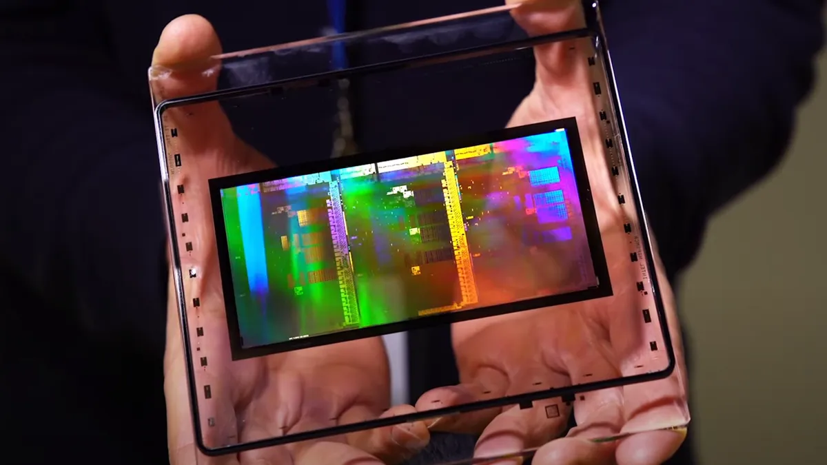
Printing the small features on a chip starts with a chunk of quartz called a photomask. This transparent quartz has an imprinted pattern of a chip design and works much like a stencil — shining a light through the mask etches the design onto the wafer, thus creating the billions of 3D transistors and wire structures that comprise a modern chip. Each chip design requires multiple exposures to build up the chip's design in layers. As such, the number of photomasks used during the chipmaking process varies based on the chip; it can even exceed 100 masks. For instance, Nvidia says it takes 89 masks to create the H100, and Intel cites '50+' masks used for its 14nm chips.

New techniques have emerged that now allow etching features smaller than the wavelength of the light used to create them. However, the continued shrinkage of the features has led to issues with diffraction, which essentially 'blurs' the design that's being printed onto the silicon. The field of computational lithography counteracts the impact of diffraction through complex mathematical operations that optimize the mask layout. However, this task is becoming increasingly compute-intensive as features shrink even further, thus enabling billions more transistors per design.

These complex problems require large clusters of computers, often numbering tens of thousands of servers (Nvidia cites 40,000), that crunch through the numbers in parallel on CPUs in a workload that can take up to weeks to process a single photomask (the amount of time varies based on chip complexity — Intel says it takes its team five days to create a single mask).

Nvidia contends that the number of servers required to design a modern mask is increasing at the same rate as Moore's Law, thus pushing the server requirements and the amount of power needed to operate them into unsustainable territory. In fact, the incredible compute requirements for new mask tech, like Inverse Lithography Technology (ILT) which uses Inverse Curvilinear Masks (ILM), has already hampered the adoption of these more advanced techniques. Additionally, High-NA EUV and ILT are expected to increase the amount of data processing for masks by 10X in the coming years.

That's where Nvidia's cuLitho steps in, reducing the computational lithography workload to eight hours. The cuLitho library can be integrated into computational lithography software that leverages ILT (curvilinear shapes) or Optical Proximity Correction (OCP, which uses 'Manhattan' shapes) techniques, and is already integrated into Synopsys' tools. TSMC and ASML are also adopting the tech. Given the sensitivity of these sorts of software, US export controls will govern any distribution of the software to China and other regions subject to sanctions.

Intel has long used its own proprietary software tools but is slowly shifting to adopting industry-standard tools, particularly as it begins implementing its own external IDM 2.0 foundry operations. As such, it is yet to be seen if other big fabs, like Intel and Samsung, will adopt the new software for their own internal tools. Regardless, the support from Synopsys, ASML, and TSMC assures broad uptake of the cuLitho library and Nvidia's GPU-based solutions with leading semiconductor manufacturers over the coming years.  

Paul Alcorn
Managing Editor: News and Emerging Tech

Paul Alcorn is the Managing Editor: News and Emerging Tech for Tom's Hardware US. He also writes news and reviews on CPUs, storage, and enterprise hardware.

  • drivinfast247
    So that means cheaper production and lower prices for consumers? Right?
    Reply
  • Jimbojan
    It is not clear NVDA lithographic is any better than Intel's. Don't expect any new design will result in cheaper process, it always costs more, from past experience.
    Reply
  • peachpuff
    drivinfast247 said:
    So that means cheaper production and lower prices for consumers? Right?
    Jensen: muwahahahahaha fools!
    Reply
  • drivinfast247 said:
    So that means cheaper production and lower prices for consumers? Right?
    Sure, if this is opposite Day
    Reply
  • InvalidError
    Jimbojan said:
    It is not clear NVDA lithographic is any better than Intel's. Don't expect any new design will result in cheaper process, it always costs more, from past experience.
    If you reduce the calendar cost of making computational lithography masks by 40X, it does save millions of dollars on the tape-out process and opens the doors for higher-precision optical modelling which should improve yields at even smaller detail resolution using an otherwise fundamentally unchanged fab process. Being able to pump new masks in a day instead of weeks also means much faster design iterations from first silicon to production, which reduces the amount of time engineers have to fill doing other stuff while waiting for silicon, which can itself reduce the amount of interim work that may get thrown away when silicon doesn't behave exactly as simulations predicted.

    Of course, based on the last three years, there is a practically zero chance Nvidia will pass any of the savings to consumers.
    Reply
  • kjfatl
    40 times faster that something that was obsolete 10 years ago?
    Doesn't everyone doing this kind of work use GPU's or a custom ASIC to do this array processing?
    It's a marketing slide. It could be faster than anything else out there or it might be the real reason that Intel is developing their own GPU family.
    Reply
  • russell_john
    drivinfast247 said:
    So that means cheaper production and lower prices for consumers? Right?

    Well not right away because first you have to earn back the cost of 500 H100 at $33,000 - $38,000 a pop or an initial investment of $16.5 million - $19 million and that doesn't begin to count the other system hardware, manpower to set it up, manpower to run it or the cost of electricity .... In other words Return on Investment will take a couple of years

    What it actually means is the Consumer Market will have to compete against the Commercial Market for production time at TSMC .... If demand is high for Nvidia's high margin commercial products and right now it definitely is because of things like this and GPT Ai then Nvidia really has no choice but to move production time over from the Consumer products to the Commercial products and if they are going to release Consumer products the margins will have to be high or it's just not worth the manufacturing time.

    Put yourself in their shoes ... You have two products one nets you $1000 in profit and the other nets you $2000 but you only have the capacity to make 1000 total units. Are you going to mainly make the $1000 profit units or the $2000 profit units?
    Reply
  • InvalidError
    kjfatl said:
    40 times faster that something that was obsolete 10 years ago?
    Computational lithography at ~3nm is practically atomic-scale reverse-raytracing to compute the lens properties needed to convert a given EUV light field into a specific projected pattern. EUV to enable this sort of resolution didn't exist 10 years ago and the amount of compute power necessary to do computational lithography at that resolution wouldn't have been economically viable. It may not even have been feasible at all until recently due to VRAM limitations.
    Reply
  • bit_user
    New techniques have emerged that now allow etching features smaller than the wavelength of the light used to create them.
    I'm pretty sure that's not true. EUV is like 10 nm, right? From what I've gleaned, the smallest actual features on modern nodes are several times that size.

    What's ironic about this is that it will almost certainly benefit AMD.

    drivinfast247 said:
    So that means cheaper production and lower prices for consumers? Right?
    Even if the price stays the same, just shortening the time to market is going to be extremely valuable.

    russell_john said:
    Well not right away because first you have to earn back the cost of 500 H100 at $33,000 - $38,000 a pop or an initial investment of $16.5 million - $19 million and that doesn't begin to count the other system hardware, manpower to set it up, manpower to run it or the cost of electricity .... In other words Return on Investment will take a couple of years
    Who said anything about buying the hardware? Nvidia will rent you time on their cloud, I'm sure. If not, then probably the partner companies mentioned in the article would be the ones to buy the GPUs, as an added value for customers. Of course, it'll cost more for said customers, if they want the fast-turnaround option.

    russell_john said:
    Put yourself in their shoes ... You have two products one nets you $1000 in profit and the other nets you $2000
    Your numbers are way off. H100 sells for like $18k, so their margins are probably at least half that. And they're certainly not making $1k profit on a RTX 4090.
    Reply
  • InvalidError
    bit_user said:
    I'm pretty sure that's not true. EUV is like 10 nm, right? From what I've gleaned, the smallest actual features on modern nodes are several times that size.
    There seems to be something missing or misphrased at the end there: I hope your "several times that size" was meant as "several times smaller" as even Intel's 14nm process which used 193nm DUV had some sub-10nm features such as 8nm fin width. Add the oxide layer between the fin and gate along with the gate itself and you get the 34nm fin pitch.

    EUV is more of the same using a 13.5nm light source to reduce the amount of multi-patterning, associated costs and yield issues.
    Reply