Synopsys' AI-Assisted EDA Tools Aim To Cut GPU Design Costs in Half
Synopsys' AI-assisted EDA tools can cut chip design time from 24 months to 24 weeks.

Get Tom's Hardware's best news and in-depth reviews, straight to your inbox.
You are now subscribed
Your newsletter sign-up was successful
At Hot Chips 2021, Synopsys announced an ambitious plan to develop a fully integrated set of electronic design automation (EDA) tools that rely on artificial intelligence. These tools promise to cut chip development costs, reduce time to market, improve performance, and boost yields. Samsung has already received its first chip designed using AI-assisted EDA tools and found that it performs better than expected while consuming less power.
Optimizing Physical Layout
Physical design of modern chips is an expensive and difficult process, and as fabrication technologies get thinner, IC design costs are escalating. Nowadays it takes years to develop a new CPU or GPU architecture and then it may easily take about 24 months or more to design physical implementation of the chip. At 3nm design cost of a sophisticated GPU will approach $1.5 billion, according to some analysts, a sum that not all companies can afford. But there is a way to cut these costs by as much as 50% and development time by orders of magnitude using AI-enabled design tools, says Synopsys.
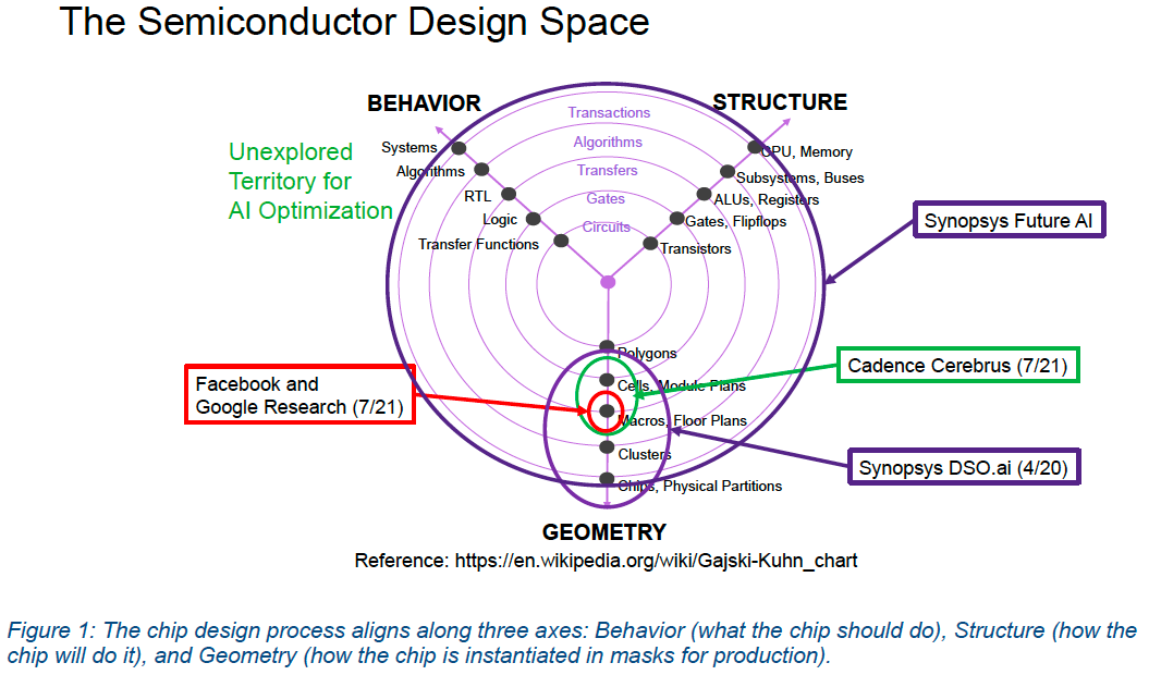
Modern EDA tools greatly simplify development of chips, but chip floorplan, layout, placement, and routing require input from human engineers that use their experience to develop efficient designs. Every small aspect of a chip design requires people to evaluate different design options and make multiple decisions. While experienced engineers tend to work fast, they cannot evaluate hundreds of design options in a reasonable amount of time, explore viability of all possible combinations and then simulate tens if not hundreds of different layouts to find the most optimal one. By contrast, the Synopsys DSO.ai platform can do just that with one noticeable exception: it does not have to simulate all the 10^90,000 possible ways to place and route an IC as it can figure out the best one using artificial intelligence.
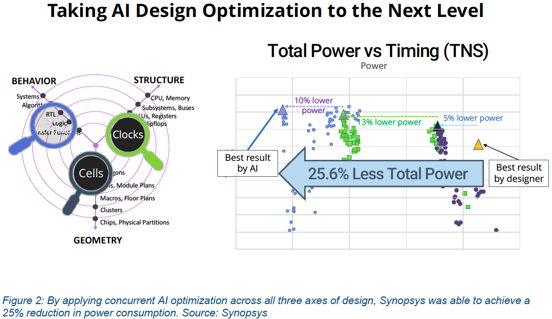
Synopsys' DSO.ai is compatible with the company's EDA tools and promises to optimize all PPA (performance, power, area) aspects of chip design in time that is impossible for human engineers today. For example, a test chip designed by Synopsys using AI-assisted software achieved a 26% power reduction when compared to the same chip designed by a human engineer and it only took the machine a fraction of time. To get there, Synopsys DSO.ai optimized geometry, architectural choice points and associated physical layouts, and behaviour of the chip.
Synopsys' DSO.ai algorithms are compatible with all process technologies, so their value will increase over time when complexities of IC design increase. Synopsys says that chip design (place and route) time can potentially decrease to 24 weeks from 24 months today because of AI usage.
Samsung was the first company to adopt the Synopsys DSO.ai platform for chip design and has already received its working IC from the fab. Google and Nvidia have also picked up DSO.ai, so expect these companies to speed up development of their chips and lower their design costs.
New Approach
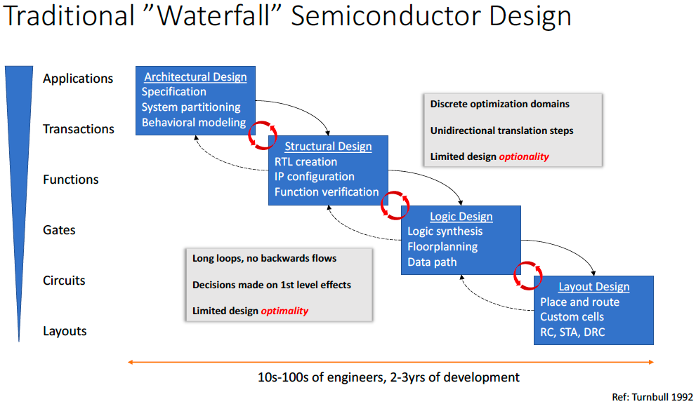
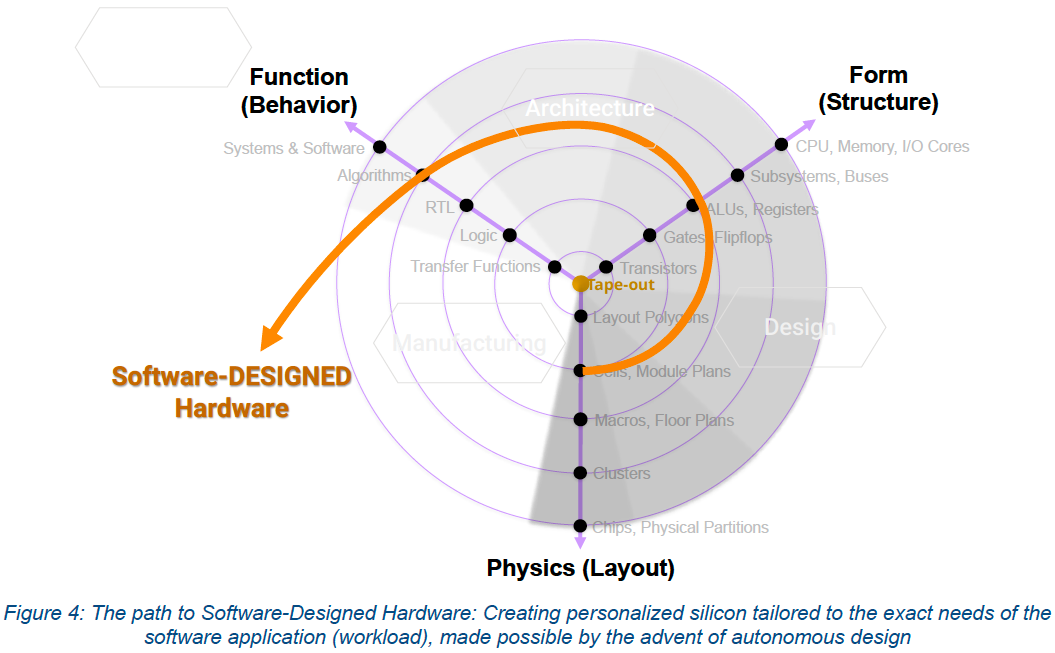
Yet physical (layout) design and floorplanning are not the only chip development steps that can take advantage of AI-assisted tools. To build an IC, developers must design architecture, structure, floorplan, and layout. Normally, creators use the so-called waterfall semiconductor design approach and develop each step separately.
Get Tom's Hardware's best news and in-depth reviews, straight to your inbox.
Synopsys says that this traditional approach has a number of drawbacks that negatively affect chip design process, making it longer (with architecture development, it takes at least three years to build a contemporary chip) as design options are not evaluated synchronously simply due to limitations of human engineers.
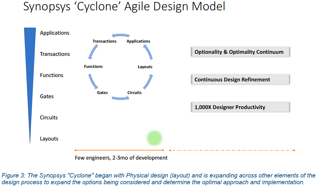
The maker of EDA tools proposes chipmakers to adopt a new cyclone design model that will involve concurrent evaluation of all key elements of a chip using AI-assisted software to optimize all aspects of a semiconductor design to get the best performance, power, and costs in a considerably shorter amount of time. Synopsys says that cyclone chip design approach could reduce chip development time to two or three months and increase designer productivity by a factor of 1,000, which will reduce the number of engineers involved in chip design.
Cutting down an SoC development time and the number of engineers required will enable small companies that currently cannot afford to develop their own processors to enter the market and offer solutions tailored for applications that presently rely on general-purpose hardware.
Synopsys admits that usage of AI-assisted EDA tools requires rather tremendous compute horsepower that does not come cheap. Big companies like Google or Nvidia have rather formidable datacenters used for simulation of architectures and circuits, so nothing will change for them. For smaller players Synopsys is mulling to offer AI-assisted tools in the cloud, which will further democratize chip design costs.
Summary
Synopsys' DSO.ai software enables chip developers to reduce power consumption, improve performance, shrink die size, and shorten development time of semiconductors. This is a big deal since physical designs are getting harder to implement and their complexity will only grow in the coming years. Since chip design costs will grow dramatically as the industry transits to 3 nm fabrication process as well as GAAFET transistors, AI-assisted EDA tools will become crucially important to developers of big chips.
Yet AI-assisted physical design tools are only a tip of the iceberg when it comes to AI in chip development. Traditional waterfall approach to semiconductor design does not allow engineers to concurrently evaluate different architectural and design options, which increase costs and time-to-market, Synopsys claims. The EDA company believes that a moly holistic cyclone design model as well as software-designed hardware will enable developers to cut down design time and costs significantly, which will open doors to chip development to companies that previously could not afford it.

Anton Shilov is a contributing writer at Tom’s Hardware. Over the past couple of decades, he has covered everything from CPUs and GPUs to supercomputers and from modern process technologies and latest fab tools to high-tech industry trends.
