Toshiba Talks 5-Bit-per-Cell Flash, Demos First PCIe 4.0 Enterprise SSDs
Toshiba Memory had quite a bit going on at the Flash Memory Summit this year. Aside from the hustle and bustle of the company’s new XFMEXPRESS form factor winning Best of Show, the company also had plenty of other leading-edge storage technology on display. With a few new PCIe 4.0 NVMe SSDs, the launch of XL-Flash Storage Class Memory (SCM), and some interesting Ethernet SSDs featuring native NVMe over fabrics (NVMe-oF), Toshiba is embracing PCIe 4.0 and new storage technologies. At the show, there was even mention of future BiCS FLASH, including Penta-level cell (PLC) NAND development.
BiCS 5, 6, & 7, and 5-bit-Per-Cell Flash…PLC to Come?
At Toshiba’s keynote, the company’s speaker discussed not only the company's XL-Flash technology but also some interesting points on future developments.
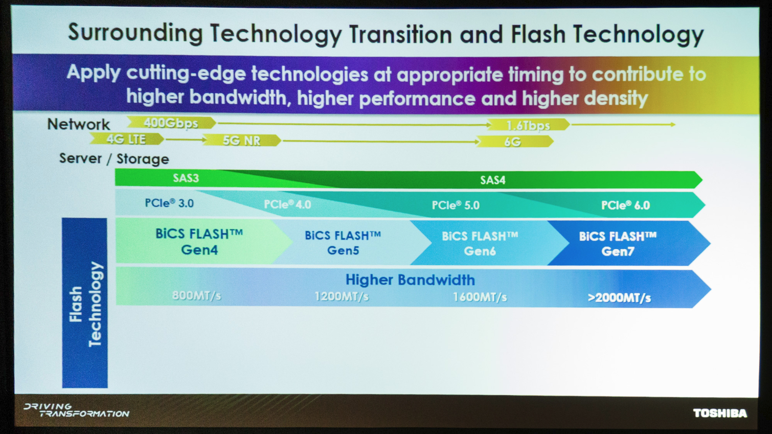
Toshiba has already begun planning the fifth through seventh generations of its BiCS Flash. Each new generation will coincide with new generations of the PCIe standard, beginning with BiCS 5 that will come to market soon in alignment with PCIe 4.0, but the company hasn't provided a specific timeline. BiCS5 will feature higher bandwidth of 1,200MT/s, while BiCS6 will hit 1,600MT/s, and BiCS7 is slated to reach up to 2,000MT/s.
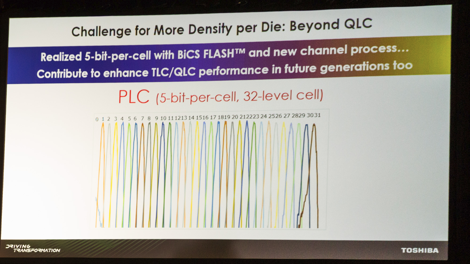
The company has also started research into Penta-level cell (PLC) NAND flash and actually verified working five-bit per cell NAND by modifying its current QLC NAND. The new flash provides more density with the ability to store five bits per cell, rather than just four in current QLC. But, to do this, the cell needs to be capable of storing 32 distinct voltage levels, and SSD controllers need to read them back accurately. With so many voltage levels to read to and write at nano-scale, the new technology is very challenging. To get control of the tighter thresholds, the company had to develop some additional processes that may adapt to its current TLC and QLC to boost performance.
QLC is already fairly slow and has lower endurance than other types of flash. PLC will have even less endurance and slower performance. New NVMe protocol features such as Zoned Namespaces (ZNS) should help mitigate some of the issues, however. ZNS by itself aims to reduced write amplification, reduce the need for media over-provisioning and internal controller DRAM usage, and of course, improve throughput and latency.
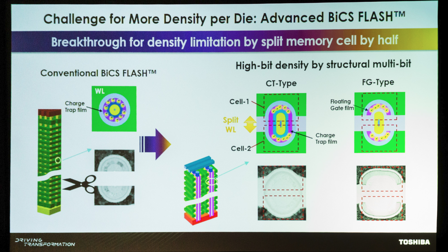
The company has developed a new process that increases die density in the next generations of BiCS FLASH in all forms. It essentially will split the memory cell in half to scale up while retaining the regular 3D flash process. Toshiba is not sure if this approach is entirely feasible at this time.
Get Tom's Hardware's best news and in-depth reviews, straight to your inbox.
XL-Flash Details, Sampling, and Production Update
Toshiba announced XL-Flash at FMS last year. XL-Flash is Toshiba’s response to Samsung’s Low Latency V-NAND (aka Z-NAND) and Intel’s Optane memory. Because Optane is so expensive and Samsung’s solution is proprietary to its branded products, Toshiba saw an opportunity design a more cost-effective, lower latency storage solution for the company’s customers that bridges the gap between DRAM and NAND performance.
Key Features:
- 128 gigabit (Gb) die (available in a 2-die, 4-die, 8-die packages)
- 4KB page size for more efficient operating system reads and writes
- 16-plane architecture for more efficient parallelism
- Fast page read and program times. Toshiba says XL-FLASH provides read latency of less than 5 microseconds, approximately 10 times faster than existing TLC
With what seems like a similar design to Samsung’s Low latency V-NAND, XL-Flash is a form of SLC NAND that has been optimized for the fastest response times. Initially, Toshiba will use the persistent memory in SSDs, but the company mentions possible use in non-volatile dual in-line memory modules (NVDIMMs) that ride on the DRAM bus. Sample devices are already built, and shipments will start in September. Toshiba expects mass production to begin in 2020.
PCIe 4.0 SSDs for Enterprise and Data Center Applications
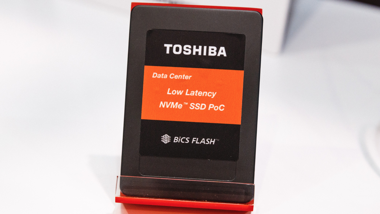
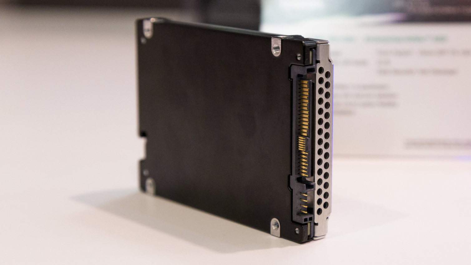
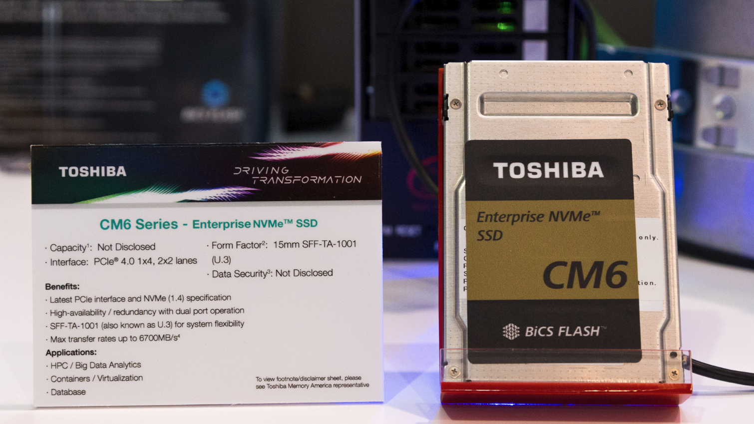
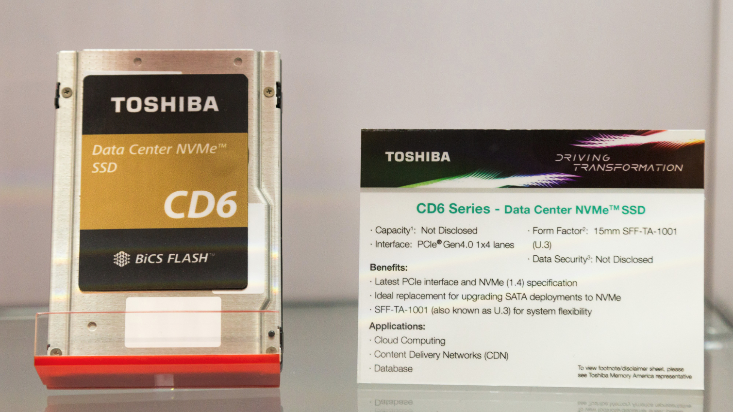
Toshiba is the first company to announce and publicly demo enterprise/data center PCIe 4.0 SSDs. Built using company’s latest 96-layer BiCS4 flash, the all-new CM6 Series enterprise and CD6 Series data center SSDs clock in at speeds of up to 6.7 GB/s of sequential throughput.
The CD6 is built for cloud computing, content delivery networks (CDNs), and database applications while the CM6 is aimed towards HPC, big data analytics, containerized, and virtualization applications. Each comes in the new U.3 form factor (SFF-TA-1001) factor and are available in single port (CD6) and single/dual port (CM6) configurations. Additionally, they support the latest NVMe 1.4 specification.
Ethernet SSDs Featuring Native NVMe over Fabrics Support
With last year’s launch of KumoScale, a software that disaggregates high-performance NVMe SSDs from compute nodes and makes them shared and available across a network infrastructure as network-attached resources, Toshiba launched its embraced NVMe-oF.
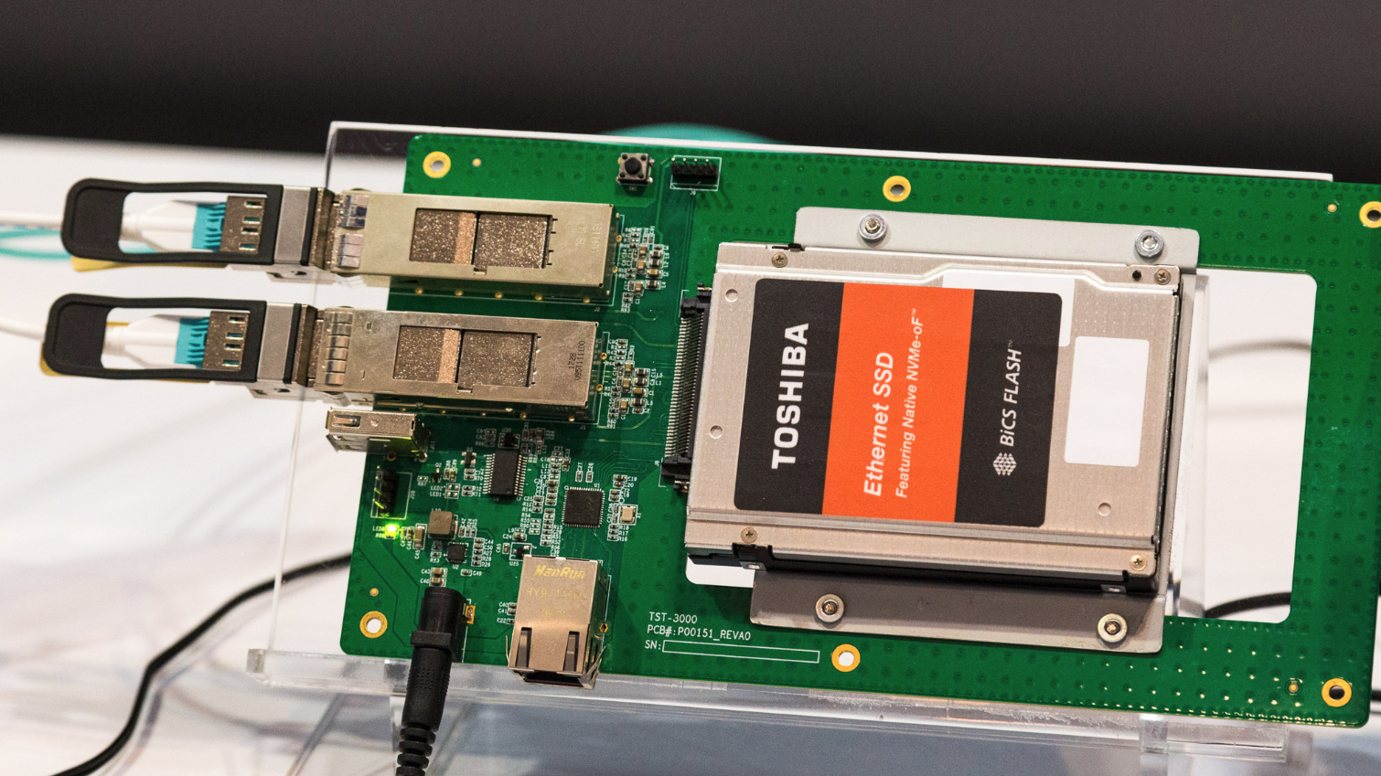
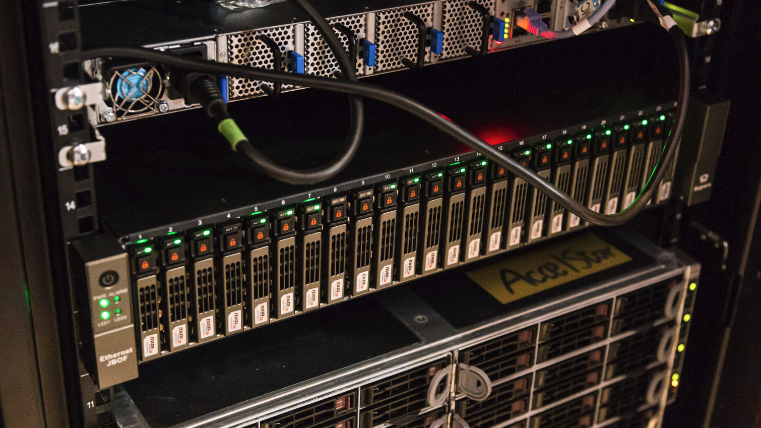
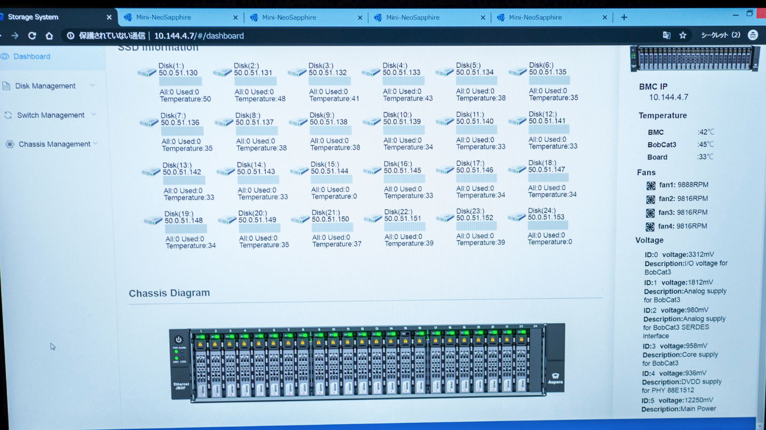
Toshiba showed off an Ethernet JBOF box packed with 24 Ethernet SSDs. Each SSD appears in the system with an individual IP address for access over Ethernet. The production-ready prototype SSDs feature Toshiba’s 96L 3D NAND and utilize Marvell 88SN2400 NVMe-oF SSD controllers to create 25Gb Ethernet links rather than PCIe lanes.
NVMe-oF is quite an interesting and useful technology. It aims to bring low latency access over the fabric and expose the entire SSD’s bandwidth to the network as well as and mitigate the need for high PCIe lane allocations for storage deployment. So, those valuable lanes can be used for more important computational devices like GPUs and other accelerator cards, rather than local storage.

Sean is a Contributing Editor at Tom’s Hardware US, covering storage hardware.
-
hannibal Better that way! You don't Waste time installing programs because the drive fails before you get that far :ROFLMAO:Reply
But yeah... don't use this for anything you have to save longer time. Maybe a space for windows temporary files and browser cookies... -
Giroro Replyrazor512 said:Awesome, a SSD that will fail before you can finish installing the Linux kernel.
Don't worry, they're going to mitigate the problem by installing your OS into your RAM.
Because the point of nonvolatile storage is to keep as much as possible in your volatile memory, right? It made me wonder how long until motherboards start shipping with backup batteries, just to keep cheap storage functional... Then I remembered that ultra-cheap unreliable SSDs are mostly being used to occupy the only m.2 slot in OEM laptops with <1yr warranties. -
bit_user ReplyPenta-level cell (PLC)
It's really incorrect to call it penta-level cells, since 5-level cells do not store 5 bits of information! The actual amount you can pack into them would be log2( 5 ) which is about 2.322 bits per cell. In practice, it would be a little lower than that, because the packing is done on a block-level, and then you need to spend some bits on ECC.
There's a slide that makes it clear they're actually talking about 32-level cells, which are truly 5-bit (before accounting for ECC overhead, etc).
The abbreviation should be PBC (Penta-Bit Cell).
Anyway, I'm hoping to buy something like their XL-Flash in a M.2 or PCIe card. -
TJ Hooker Reply
I agree, but to be fair at this point they're essentially just following the (bad) convention started with TLC (and then QLC). Which in turn were probably trying to stick to the format of LC as started by MLC, which was a more or less appropriate acronym (or at least was until it started being used to refer specifically to 2 bit-per-cell NAND). What a mess lol.bit_user said:It's really incorrect to call it penta-level cells, since 5-level cells do not store 5 bits of information!
The abbreviation should be PBC (Penta-Bit Cell). -
bit_user Reply
Eh, they don't necessarily need to adopt PLC,at this time, even though Toshiba used it in a slide.TJ Hooker said:I agree, but to be fair at this point they're essentially just following the (bad) convention started with TLC (and then QLC). Which in turn were probably trying to stick to the format of LC as started by MLC, which was a more or less appropriate acronym (or at least was until it started being used to refer specifically to 2 bit-per-cell NAND). What a mess lol.
