TSMC's 16FF+ Process Reaches Risk Production Milestone; Mass-Production Planned For Mid-2015
Get Tom's Hardware's best news and in-depth reviews, straight to your inbox.
You are now subscribed
Your newsletter sign-up was successful
TSMC's FinFET-based 16FF+ process has reached the risk production milestone. The new process promises to increase the chips' performance by 40 percent compared to the 20nm process, but at the same power consumption level. (Or it can cut power consumption in half, if performance is maintained at similar levels.)
"The 16FF+ process offers customers a new level of performance and power optimization targeted at the next-generation of high-end mobile, computing, networking and consumer applications," TSMC said.
This new process should allow Cortex A57 chips to reach 2.3 GHz for high-speed applications and Cortex A53 chips to consume as little as 75mW for low-end tasks. A gain of roughly 15 percent in performance or area efficiency is expected over the 16FF process.
Article continues below"Our successful ramp-up in 20SoC has blazed a trail for 16FF and 16FF+, allowing us to rapidly offer a highly competitive technology to achieve maximum value for customers' products," said Mark Liu, president and Co-CEO for TSMC. "We believe this new process can provide our customers the right balance between performance and cost so they can best meet their design requirements and time-to-market goals."
TSMC's 16FF+ process is about to pass its full reliability qualification later this month, and it should be ready to make chips that ship into devices next year. TSMC claimed that it already has 60 design wins that are expected to tape-out by the end of 2015. The company expects mass production of 16FF+ chips to start in July 2015.
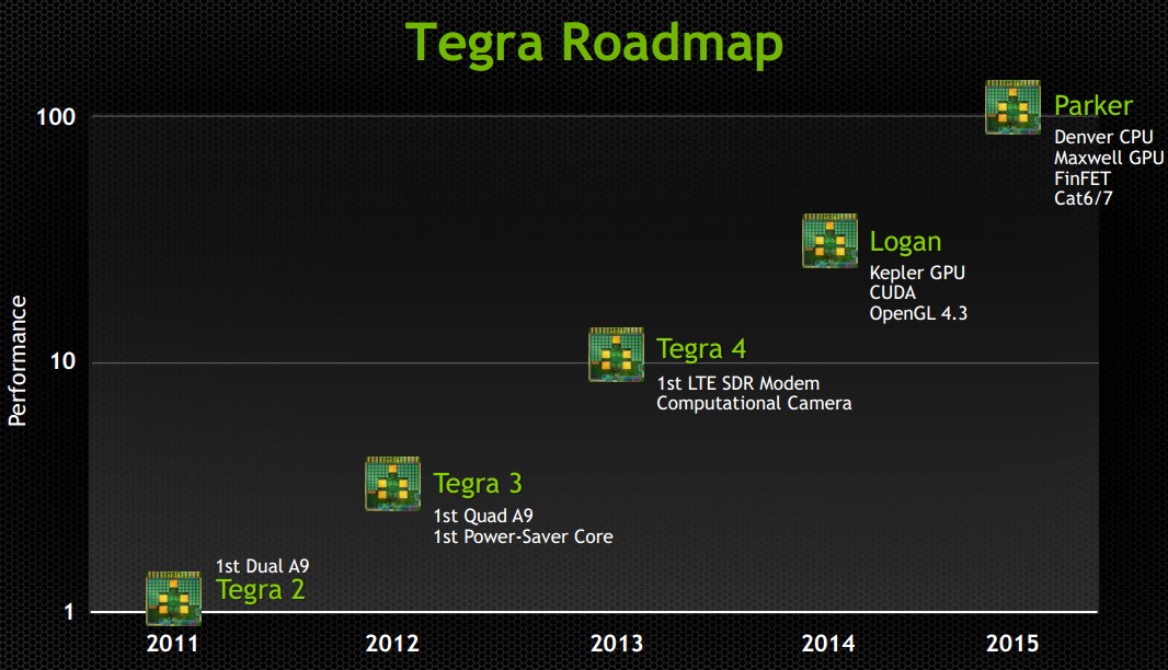
Nvidia has already promised that it will be using a "16nm FinFET" process for its Maxwell-based Tegra chip next year, which implies a TSMC process but doesn't say whether it will be the 16FF process or the 16FF+ one. Nvidia doesn't usually pick the most cutting edge process available, so unless the company decides to surprise us, it will probably be the former.
Apple has mainly gone with TSMC's 20nm processor for its chips this year, but it's unclear whether it will stick with TSMC or move back to Samsung's 14nm process. Either way, it seems like 2015 will be the year of FinFETs, when most chip makers can finally adopt FinFET transistors in their chips for lower leakage, higher-driving current, lower-voltage operations and higher intrinsic gains.
Get Tom's Hardware's best news and in-depth reviews, straight to your inbox.
Follow us @tomshardware, on Facebook and on Google+.
Lucian Armasu is a Contributing Writer for Tom's Hardware US. He covers software news and the issues surrounding privacy and security.

