TSMC Might Bring 3nm Production to U.S.
TSMC is already building second phase of Arizona fab

Taiwan Semiconductor Manufacturing Co. could bring production of chips on its leading-edge N3 (3nm-class) fabrication technology to its Arizona camp as part of its expansion, according to a report by Reuters. The company is already building a fab shell at the site and, if it thinks there is enough demand for N3 in the U.S., will install appropriate production relatively quickly.
"In light of the strong customer demand we are seeing in TSMC's advanced technology, we will consider adding more capacity in Arizona with a second fab based on operating efficiency and cost economic considerations," TSMC said in a statement to Reuters.
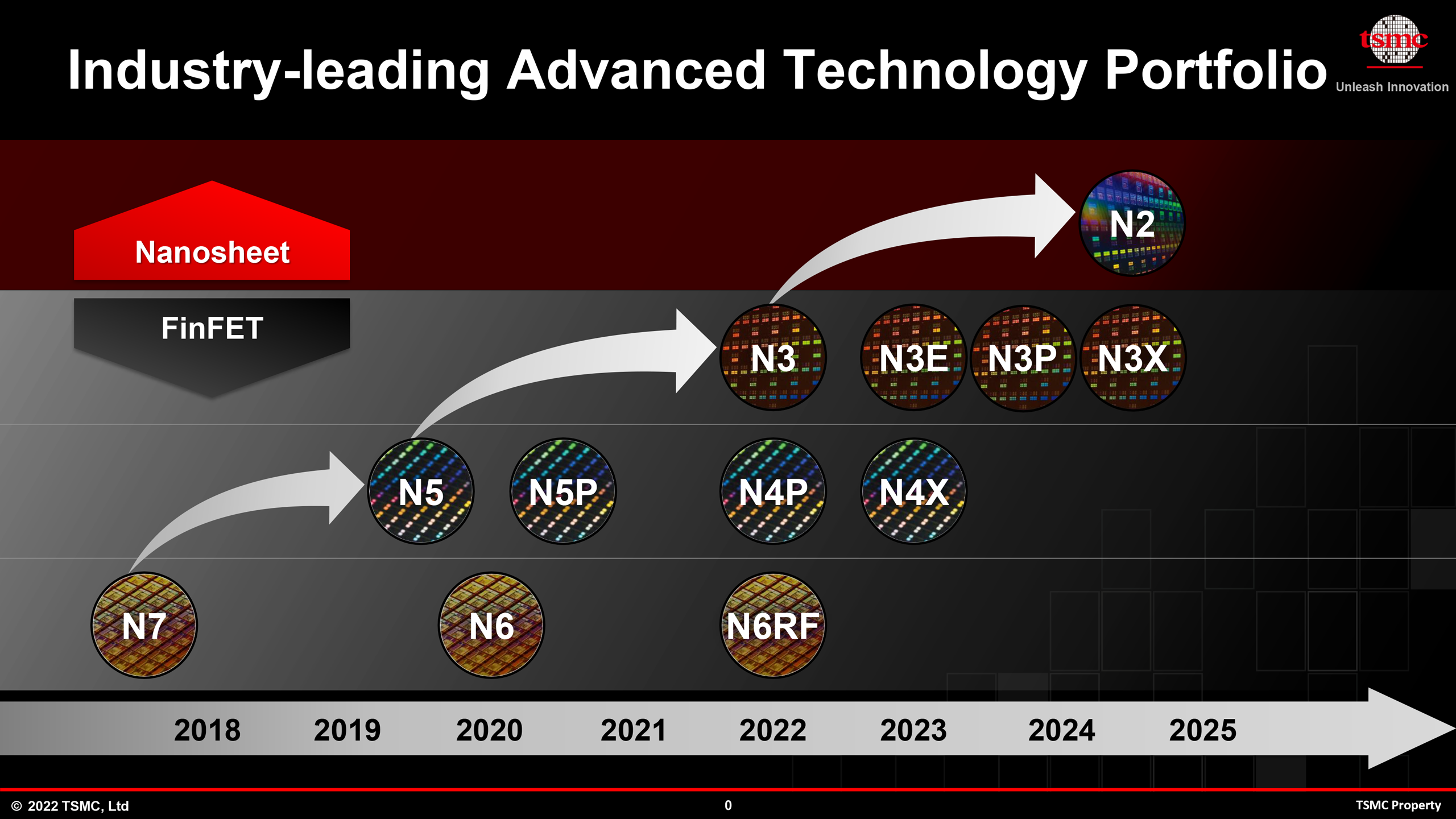
The Wall Street Journal, citing "sources familiar with the matter," claims that TSMC is considering equipping the new building with tools advanced enough to make chips on the foundry's leading-edge fabrication technologies from its N3 family, which includes N3, N3E, N3P, N3S, and N3X.
When TSMC establishes a new site for a fab, it buys enough land to build multiple phases of this fab, which will share common fab utilities such as gas storage or water purifiers. This is the case with the foundry's Arizona camp, which can host up to six fab buildings (phases) and which currently accommodates one topped-out fab that will come online in 2024. But apparently the company is already building a shell for another one.
Keeping in mind that companies based in the U.S. design around 47% of chips sold worldwide, and that the vast majority of chips made using advanced manufacturing technologies are developed by American companies, demand for TSMC's services in the U.S. is expected to be strong.
| Row 0 - Cell 0 | N3E vs N5 | N3 vs N5 |
| Speed Improvement @ Same Power | +18% | +10% ~ 15% |
| Power Reduction @ Same Speed | -34% | -25% ~ -30% |
| Logic Density | 1.7x | 1.6x |
| HVM Start | Q2/Q3 2023 | H2 2022 |
Whether it will be strong enough to bring N3 to the U.S. in the next couple of years remains to be seen. But because there are a bunch of U.S.-based companies planning to use N3 nodes in the coming years (AMD, Apple, Intel, MediaTek, Nvidia, Qualcomm, just to name a few), it certainly makes sense for the company to expand its N3 production capacity in general.
If TSMC proceeds with its N3-capable fab in the U.S., the facility will likely come online in late 2024 — or, more likely, early 2025. The foundry plans to start production on its N2 (2nm-class) process technology in the second half of 2025.
Get Tom's Hardware's best news and in-depth reviews, straight to your inbox.
Therefore, while the Arizona site might get N3, TSMC's fabs in Taiwan will still be somewhat more advanced. But the gap between TSMC's capabilities in Taiwan and the U.S. will likely shrink in the coming years (though this is our speculation rather than the foundry's official plan).

Anton Shilov is a contributing writer at Tom’s Hardware. Over the past couple of decades, he has covered everything from CPUs and GPUs to supercomputers and from modern process technologies and latest fab tools to high-tech industry trends.
-
JamesJones44 These increases in speed and efficiency have become depressing small. 18% and 25% from a node shrink is small by historic standards. Sad to think we must be getting close to peak silicon.Reply -
Eximo First transistor did not use silicon, but germanium and gold if I recall.Reply
Integrated circuits are not that old though. Earliest examples were used in the space program in the mid to late 60s. Everything prior was made with discrete transistors and consumer electronics continued that trend for another decade. (See transistor radios for good examples of the latest in consumer electronics at the time)
Personal computer's were barely a thing in the early 80s. So these more recent integrated circuit process nodes have slowed down a lot in only 40 years.
But there are workarounds. You can already see it with AMD's 3D V-cache, and HBM memory stacking. Chiplets make production more efficient and universal interconnects will make having multiple chiplets have less of an impact when it comes to latency vs a monolithic design.
There are certainly already parts of the circuits that have gotten as small as they can be. Only the dense transistor areas are nearly as small as the advertised node numbers (which you can take with a huge grain of salt) They really need to adopt that LMC metric to make chips more comparable. -
kjfatl The concept of a field-effect transistor (FET) was first patented by Austro-Hungarian physicist Julius Edgar Lilienfeld in 1925 and by Oskar Heil in 1934, but they were unable to build a working practical semiconducting device based on the concept.Reply -
kjfatl I have a textbook published in 1955 on Transistor Theory and Application. It's interesting reading. Needless to say, we have come a long way.Reply
