TSMC Outlines 3nm Roadmap: Five FinFlex Nodes
TSMC's N3 node looks to have a big and bright future with FinFlex.

As pathfinding, research, and development cycle for all-new manufacturing technologies stretches, foundries have to introduce revamped versions of their nodes in a bid to meet client requirements. TSMC on Thursday formally unveiled its N3 (3nm class) family of fabrication processes that will be used to build leading-edge chips in the next three years. One of the key features of N3 is FinFlex technology that gives chip designers additional ways to optimize performance, power, and die size.
Five 3nm Nodes
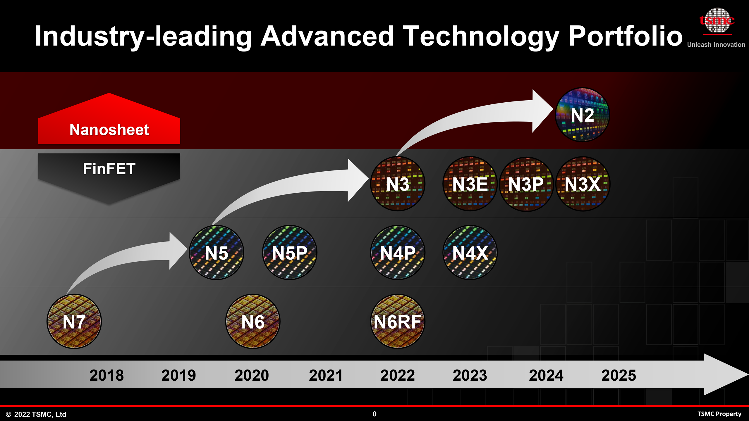
TSMC's N3 family of process technologies will consist of five nodes in total, all of which will support FinFlex. The lineup includes the original N3, set to enter high-volume manufacturing (HVM) later this year, with the first chips set to be delivered in 2023; N3E with performance-per-watt and process window improvements; N3P with additional performance enhancements; N3S with increased transistor density, and N3X with support for increased voltages, enhanced power deliver; and augmented clock rate potential for ultra-high-performance applications.
Just like TSMC announced, it will start making chips on its original N3 node later this year. This process technology is largely designed for early adopters from mobile and high-performance computing (read ASICs, CPUs, GPUs, etc.) industries that develop expensive chips (or chips for expensive devices), benefit from all kinds of performance, power, and area (PPA) improvements, and are willing to pay for them.
The original N3 node appears to have a relatively narrow process window, which may translate into lower-than-expected yield for certain applications. As a result, TSMC is prepping N3E node, which improves process window (and therefore increases yields) and also increases performance by 18% (at the same power and complexity) as well as lowers power by 34% (at the same speed and transistor count) compared to N5. Essentially, N3E enables faster and more energy efficient chips, but at the cost of slightly lower transistor density. N3E will enter risk production in the coming weeks, so it will be ready for HVM in mid-2023.
| Row 0 - Cell 0 | N3E vs N5 | N3 vs N5 |
| Speed Improvement @ Same Power | +18% | +10% ~ 15% |
| Power Reduction @ Same Speed | -34% | -25% ~ -30% |
| Logic Density | 1.7x | 1.6x |
| HVM Start | Q2/Q3 2023 | H2 2022 |
Going forward, TSMC will introduce performance-enhanced N3P for applications that need higher clocks (e.g., CPUs) and transistor density-optimized N3S process technologies for chips that benefit from more transistors (e.g., AI accelerators, GPUs, ASICs, etc.). These nodes are expected to be available in 2024. Meanwhile, by 2025, TSMC will have N3X, a very special node that will support extreme voltages, high drive currents, and will enable ultra-high-performance chips, such as processors. It looks like N3X will offer an enhanced back-end-of-line (BEOL) to improve power delivery, though we are speculating.
Ultimate Flexibility
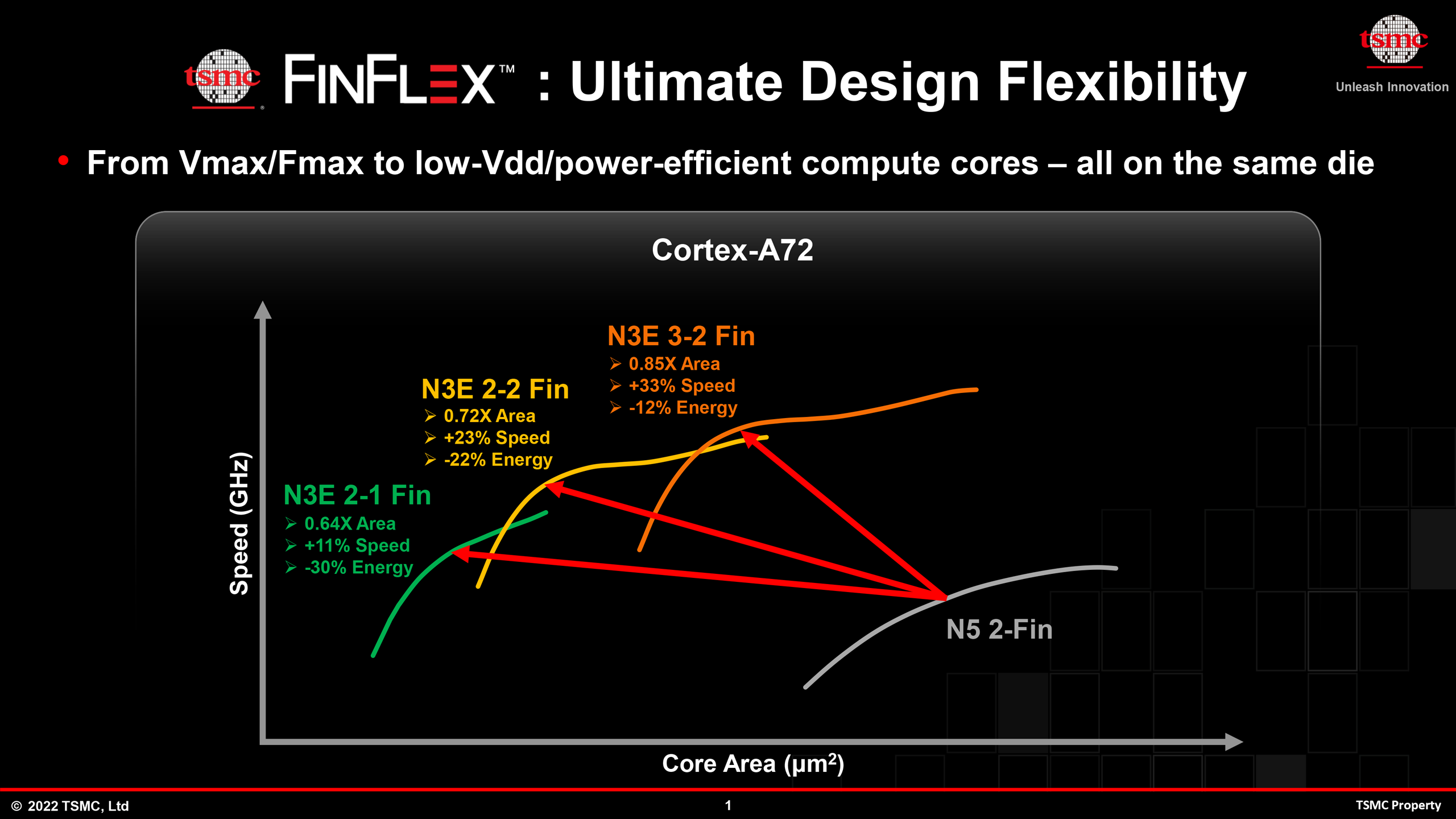
One of the things that will differentiate TSMC's N3 from other foundry nodes is the company's FinFlex technology. FinFlex should enable chip developers to balance performance, power consumption, and area with exceptional granularity.
When designing a system-on-chip, nowadays developers have to pick up one library / transistor type for each block within an SoC. For example, they can use double-gate single-fin (2-1) FinFETs to reduce die size and power consumption; they can choose dual-gate dual-fin (2-2) transistors if they want to balance performance, area, and power; or they can pick triple-gate dual-fin (3-2) FinFETs for maximum performance, but this will mean additional power consumption and die size. This is not optimal for all cases, so with N3 and FinFlex, SoC designers will be able to mix and match different kinds of FinFETs within each SoC block. This will enable experienced development teams to create exclusive configurations that will offer a unique PPA balance to meet their goals.
Get Tom's Hardware's best news and in-depth reviews, straight to your inbox.
FinFlex is not a replacement for customized / optimized nodes or even specialized libraries as nodes and libraries include much more just different FinFET configurations. But FinFlex will be particularly useful for power, performance, and costs optimizations going forward. TSMC says that FinFlex is supported by its electronic design automation (EDA) partners, so taking advantage of this capability should be relatively easy. Meanwhile, once AI-enabled EDA tools gain support for FinFlex, the latter will become even more useful.
Truth to be told, old school CPU creators adjusted their designs on transistor levels to maximize their performance, but such methodology was abandoned years ago when microprocessors got extremely complex. With FinFlex being supported by leading EDA programs, it should be easier for chip developers to use unique FinFET configurations to introduce unique optimizations and hit their design targets.
Adjusting transistor configurations for higher performance, lower power, and optimizing area is a feature that gate-all-around (GAA) transistors support by design. Enabling the mixing and matching of different FinFETs within a block could increase competitiveness of TSMC's N3.

Anton Shilov is a contributing writer at Tom’s Hardware. Over the past couple of decades, he has covered everything from CPUs and GPUs to supercomputers and from modern process technologies and latest fab tools to high-tech industry trends.

