
A recently formed company spun off from Lancaster University’s Physics Department, QuInAs Technology has one goal: develop and commercialize UltraRAM, a revolutionary new chip tech. And for the first time, Tom's Hardware was exclusively allowed to see the actual UltraRAM memory chips in a test vehicle at the company's lab at Lancaster University in Lancashire, England.
This potentially disruptive tech is designed to blend the non-volatility of flash storage with faster-than-DRAM speeds. The memory retains data even after power is removed, and the company claims it has at least 4,000X more endurance than NAND and can store data for 1,000+ years. It is also designed to have 1/10th the latency of DRAM and be more energy efficient (by a factor of 100X) than DRAM fabricated on a similar node, drawing the interest of industry heavyweights like Meta.
The last time we reported on UltraRAM was back in January 2022. Since that time, QuInAs technology has continued to develop, refine, and test the new memory. But over recent months, the biggest changes have come on the business side of things – which is vital for any startup wanting to bring their tech to market.
Lancaster Labs Tour
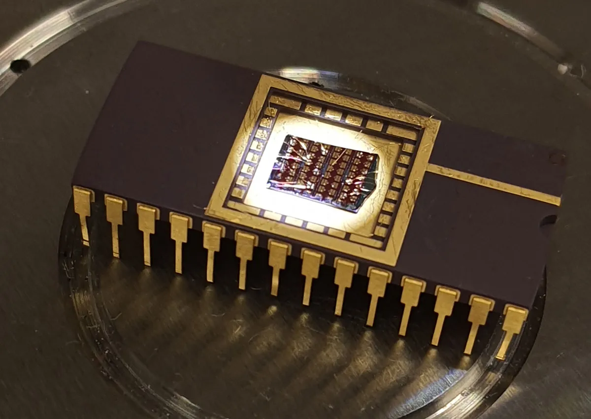
We were given a tour of the UltraRAM lab to get a first-hand look at the Physics Department’s semiconductor equipment, discuss the various fabrication techniques available at the lab, and discuss the equipment's capabilities and limits. We were also shown a working prototype of the memory riding on a test vehicle.
The best technology available at the lab will help the researchers create UltraRAM devices with features as small as 20nm. Progress to this point will take place over the next few months, and some expensive new testing and verification equipment will arrive shortly to assess UltraRAM scaling efforts.

Another important part of the lab tour was looking at a technology central to UltraRAM’s unique proposition. We looked at the MBE (Molecular Beam Epitaxy) equipment, which precisely deposits the semiconductor layers (GaSb, InAs, and AlSb) required by UltraRAM technology.

The Technology Behind UltraRAM
A triple-barrier resonant tunneling (TBRT) structure is key to UltraRAM’s advances. This highly resistive structure plays a similar role to flash NAND’s oxide layer but, according to the Lancaster University team, can facilitate data storage for 1,000+ years.
UltraRAM is a charge-based memory that uses a floating gate, like flash NAND. Also like flash, the charge state of the floating gate is read non-destructively by measuring the conductance of an underlying ‘channel.’ However, unlike flash, UltraRAM doesn't wear during program and erase cycles because of its TBRT structure.
This is a major qualifier for the durability claims of 10 million write/erase cycles, and the researchers behind UltraRAM are confident enough to claim future testing is expected to see this durability estimate revised upwards. Meanwhile, mainstream TLC 3D NAND might see gate degradation after a few thousand writes.


Another key claim about UltraRAM is that the floating gate can be switched “extremely quickly and with very little energy,” again these attractive qualities are due to the quantum mechanical phenomenon of resonant tunneling. The benefits are claimed to include UltraRAM’s 100x lower switching energy than DRAM on the same node (1,000x lower than NAND). Moreover, the UltraRAM researchers asserted that the new memory tech is expected to be capable of 1ns write operations, which is about 10x faster than DRAM.
Business Boosters
Two major events have helped QuInAs feel more confident of UltraRAM’s eventual commercial success. Firstly, at the Flash Memory Summit in August, UltraRAM won an award for the “Most Innovative Flash Memory Startup.” We heard that those interested in the future of the technology at the Santa Clara event included Meta (Facebook), who were particularly interested in the UK memory startup's power-saving claims.
Secondly, QuInAs has gained significant financial backing via an ICURe Exploit grant from Innovate UK. The funding win will soon be announced in full by QuInAs, but we know that it was awarded for demonstrating commercial viability and leading-edge science over an intensive six-month program.
With the funding rubber-stamped, the UltraRAM developers are committed to the following:
- To test nanometer scale UltraRAM devices for further proving up of claims regarding performance, efficiency, and durability.
- To cooperate with investors and move towards small volume production.
The wheels of business have certainly been in motion in recent months with the formation of QuInAs. Moreover, earlier this month, a government-sponsored UK Pavilion exhibition at SEMICON Taiwan 2023 was useful for discussions with potential technology and manufacturing partners. We gleaned from our talks with QuInAs that they might find manufacturing partners in Taiwan instead of Europe (IMEC, Belgium).

What Next for UltraRAM and QuInAs Technology?
QuInAs is about to set off on a one-year plan in line with the stated funding goals of both technical and commercial progress.
Better testing machinery is on the way to help with key process scaling and refinement steps. Moreover, IIT Roorkee in India will work as a partner to model UltraRAM performance in wider contexts. This collaboration should help develop the technology and help steer it towards its full potential.
As with all new memory technologies, the challenges of producing the new memory economically in large-scale production will prove to be a key hurdle. On the topic of the first markets for UltraRAM, QuInAs Technology is leaving options open for now, as impending work will shine a clearer light on strengths and any possible weaknesses. It seems that if all goes to plan, the initial small production runs will be targeted at the top of the memory pyramid, as it is the most lucrative segment to address.
