13 Years of Nvidia Graphics Cards
Get Tom's Hardware's best news and in-depth reviews, straight to your inbox.
You are now subscribed
Your newsletter sign-up was successful
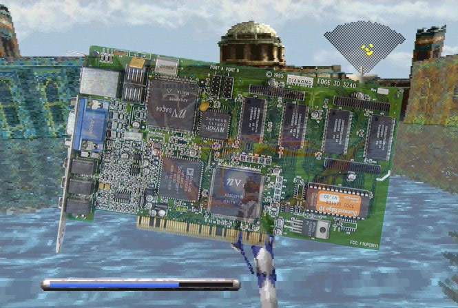
Nvidia’s history begins with the NV1 chip, sold by SGS-THOMSON Microelectronics as the STG-2000. That board included a 2D card, 3D accelerator, sound card, and a port for Sega Saturn game controllers—all on the same PCI board. The best-known of these cards is the famous Diamond Edge 3D, released two years after Nvidia’s inception.
The principal problem with the NV1 was in its management of 3D: it used quadratic texture mapping (QTM) instead of the technique used currently, which is based on polygons. DirectX appeared just after the card was released, and it used polygons, so the NV1 was a failure over the long term. Among the points worth mentioning are that the memory of the graphics card could be increased on certain models (from 2 MB to 4 MB) and that many of the games optimized were ported from the Saturn, since the card used a similar architecture.
| Date released | September 1995 |
| Card interface | PCI |
| Fillrate | 12 Mtexels/s |
| DirectX version | - |
| Memory Type | EDO/VRAM |
| Maximum memory | 4 MB |
| Memory clock frequency | 75 MHz |
| Memory bus | 64 bits |
| Maximum bandwidth | 0.6 GB/s |
| Maximum resolution | 600 x 1 200 / 15 bits |
| Video out | 1 x VGA |
| RAMDAC | 170 MHz |
The NV2 used the same rendering method and was never completed. It was to have been used in the Dreamcast console (which replaced the Saturn), but Sega finally chose a polygon-based technology (PowerVR) and Nvidia abandoned QTM in favor of polygon-based rendering with the NV3.
Riva 128 And Direct3D
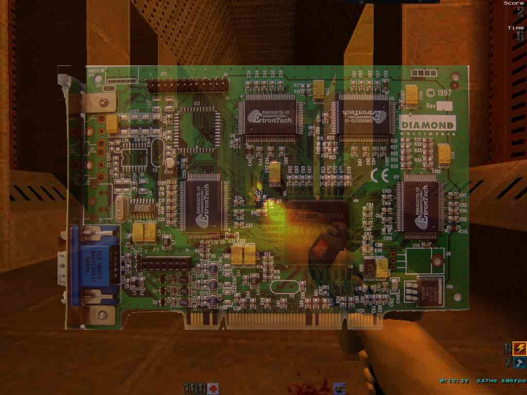
In 1997, Nvidia’s move to polygon-based 3D yielded the NV3, better known under the name Riva 128. Little known fact: Riva stands for Real-time Interactive Video and Animation accelerator. Two versions of the chip existed: Riva 128 and Riva 128ZX. The difference was slight — the ZX had a faster RAMDAC, 8 MB instead of 4 MB of memory, and AGP 2x support. The Riva 128 enjoyed a certain level of success because its price was attractive, despite quality that sometimes left a bit to be desired compared to the 3Dfx products of the period. The Nvidia card offered 2D and 3D on the same card, as well as support for Direct3D. The OpenGL drivers were released only with the 128ZX, though specific Quake versions existed (though not a complete ICD).
| Date released | April 1997 | March 1998 |
| Card interface | PCI/AGP 1x | PCI/AGP 2x |
| Fillrate | 100 Mtexels/s | 100 Mtexels/s |
| Fillrate | 100 Mpixels/s | 100 Mpixels/s |
| Rendering pipelines | 1 | 1 |
| Texture units | 1 | 1 |
| Chip clock frequency | 100 MHz | 100 MHz |
| Fabrication process | 0.35 µ | 0.35 µ |
| Number of transistors | 3.5 million | 3.5 million |
| DirectX version | 5 | 5 |
| Memory Type | SDRAM | SDRAM |
| Maximum memory | 4 MB | 8 MB |
| Memory clock frequency | 100 MHz | 100 MHz |
| Memory bus | 128 bits | 128 bits |
| Maximum bandwidth | 1.6 GB/s | 1.6 GB/s |
| Video out | 1 x VGA | 1 x VGA |
| RAMDAC | 206 MHz | 250 MHz |
The Riva 128 was popular with OEMs due to its price, which was below that of a Voodoo Graphics card and provided Direct3D performance that was nearly the same. This was one of the first AGP cards, even if the Riva 128 used the interface essentially as a faster PCI bus. Finally, and somewhat amusingly, a very well known manufacturer was a competitor of Nvidia’s for performance with one of its graphics cards: Intel, with its i740. Times have changed.
NV4: Twin Texels For The TNT
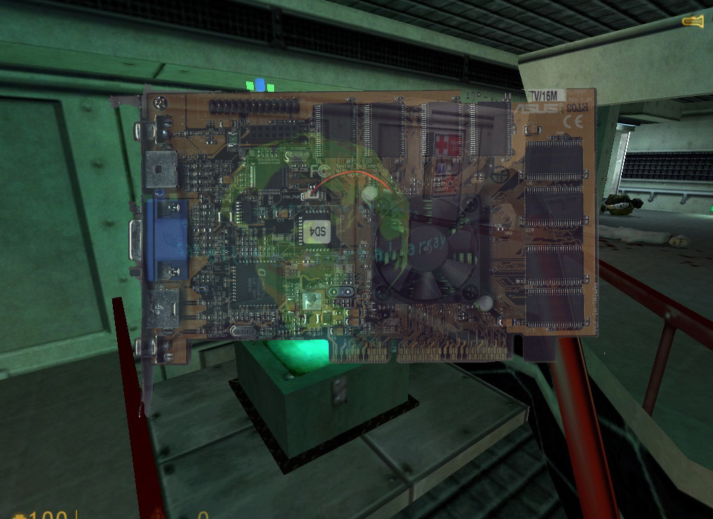
In 1998, 3Dfx had a high-performance 3D card in the Voodoo2, but the card had major limitations. These included archaic memory management (separate textures), a 16 bit color ceiling, the need for a separate 2D graphics card, and PCI-only interface (in practice, though AGP models did exist). Then the Riva TNT arrived on the scene, which was a fast 3D card with a lot of memory (for the time) and built-in 2D capabilities. Except for video performance — it had no MPEG2 acceleration, as ATI’s cards did — the TNT was a success. It was the first Nvidia card capable of applying two textures in a single pass, thus the name TNT for “TwiN Texel”.
| Date released | 1998 |
| Card interface | PCI/AGP 2x |
| Fillrate | 180 Mtexels/s |
| Fillrate | 180 Mpixels/s |
| Rendering pipelines | 2 |
| Texture units | 2 |
| Chip clock frequency | 90 MHz |
| Fabrication process | 0.35 µ |
| Number of transistors | 7 million |
| DirectX version | 6 |
| Memory Type | SDRAM |
| Memory | 16 MB |
| Memory clock frequency | 110 MHz |
| Memory bus | 128 bits |
| Maximum bandwidth | 1.75 GB/s |
| Video out | 1 x VGA |
| RAMDAC | 250 MHz |
The TNT was a less powerful card than originally planned. Nvidia had wanted to bring out a faster card than the Voodoo2, using a 250 nm process with a clock speed of 110 MHz (200 MHz for the memory). In fact, the TNT used a 350 nm process and had a clock speed of 90 MHz, like the 3Dfx card, with the memory running at 110 MHz.
NV5: The First Ultra
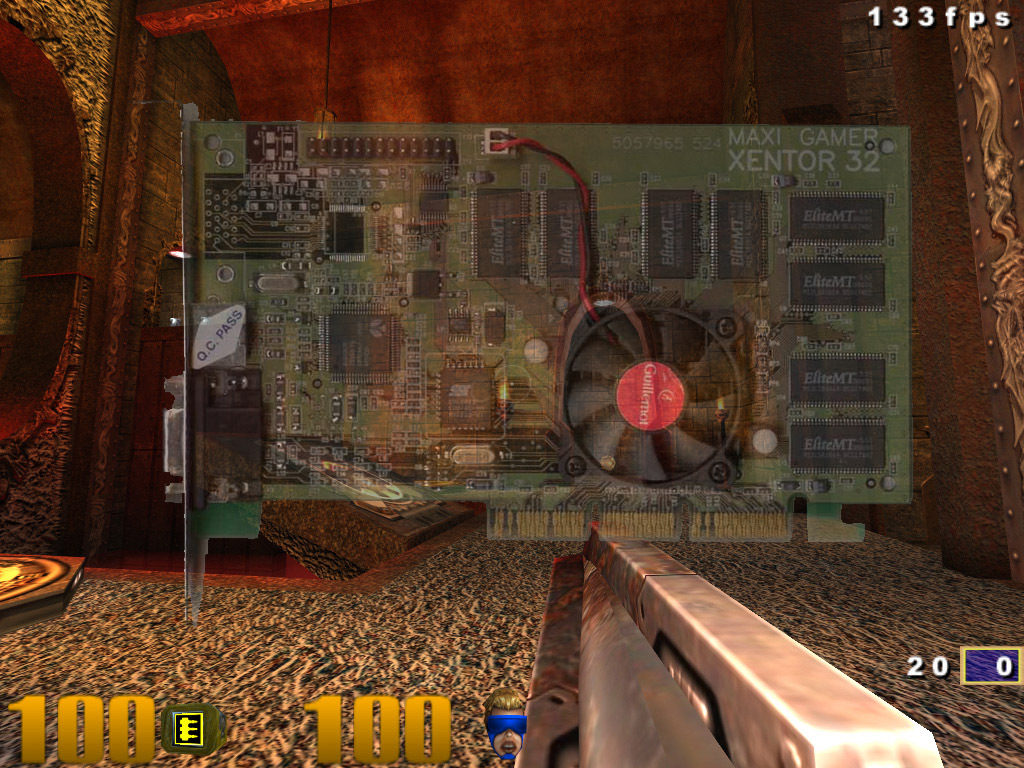
In 1999, the TNT2 made its appearance. It was close to what the TNT was originally supposed to be, and can be thought of as a die shrink of the TNT from 350 to 250 nm. This was also the first time Nvidia used the name Ultra for one of its cards.
The TNT2 cards were segmented in terms of frequency. At the time, Nvidia used only two versions (far from today’s bewildering assortment): TNT2 and TNT2 Ultra. The TNT2 was a powerful card for its time, easily a match for the Voodoo3 while offering more features, even though there was still no MPEG2 decoding. It was also Nvidia’s first AGP 4x card, even though that standard wasn’t really used with the TNT2.
Get Tom's Hardware's best news and in-depth reviews, straight to your inbox.
| Date released | March 1999 | March 1999 |
| Card interface | PCI/AGP 4x | PCI/AGP 4x |
| Fillrate | 250 Mtexels/s | 300 Mtexels/s |
| Fillrate | 250 Mpixels/s | 300 Mpixels/s |
| Rendering pipelines | 2 | 2 |
| Texture unit | 2 | 2 |
| Chip clock frequency | 125 MHz | 150 MHz |
| Fabrication process | 0.25 µ | 0.25 µ |
| Number of transistors | 15 million | 15 million |
| DirectX version | 6 | 6 |
| Memory Type | SDRAM | SDRAM |
| Memory | 32 MB | 32 MB |
| Memory clock frequency | 150 MHz | 183 MHz |
| Memory bus | 128 bits | 128 bits |
| Maximum bandwidth | 2.4 GB/s | 2.9 GB/s |
| Video out | 1 x VGA | 1 x VGA |
| RAMDAC | 300 MHz | 300 MHz |
The NV6, which also came out in 1999, was a cut-down version of the TNT2. It was sold under the name Vanta, Vanta LT and TNT2 M64. These cards were significantly slower than the TNT2 (and the original TNT), essentially because of their lower clock frequency and 64-bit memory bus. They were very successful with OEMs, however, who used the name “TNT2” as bait.
GeForce: The First GPU
Late in 1999, Nvidia announced the GeForce 256. This was the first card to use what Nvidia called a “GPU,” but its major advance was really consumer hardware support for T&L (transform and lighting). This technology, already being used in Open GL and in professional 3D, performs calculations on triangles on the graphics card instead of on the CPU. The actual gain was considerable in certain cases, since the graphics card had approximately four times the power of a high-end CPU of the time (15 million triangles for the GeForce, as opposed to four million on a 550 MHz Pentium III).
The card used a different architecture from the TNT2. Instead of two rendering pipelines, each equipped with a texture unit, there were four pipelines with one texture unit, which gave the GeForce more rendering power at a lower clock frequency. The GeForce 256 was also the first card to use DDR SDRAM, increasing memory bandwidth.
| Date released | October 1999 | February 2000 |
| Card interface | PCI/AGP 4x | PCI/AGP 4x |
| Fillrate | 480 Mtexels/s | 480 Mtexels/s |
| Fillrate | 480 Mpixels/s | 480 Mpixels/s |
| Rendering pipelines | 4 | 4 |
| Texture unit | 4 | 4 |
| Chip clock frequency | 120 MHz | 120 MHz |
| Fabrication process | 0.22 µ | 0.22 µ |
| Number of transistors | 23 million | 23 million |
| DirectX version | 7 | 7 |
| Memory Type | SDRAM | DDR |
| Maximum memory | 32 MB | 32 MB |
| Memory clock frequency | 166 MHz | 150 MHz (x2) |
| Memory bus | 128 bits | 128 bits |
| Maximum bandwidth | 2.6 GB/s | 4.8 GB/s |
| Video out | 1 x VGA | 1 x VGA |
| RAMDAC | 350 MHz | 350 MHz |
| Video playback | MPEG2 semi-hardware | MPEG2 semi-hardware |
Nvidia moved directly from NV6 to NV10 for the GeForce 256, and the nomenclature of the following models was in steps of five, with variants for the low/high-end models. Also, the GeForce 256 was the first Nvidia card to handle MPEG2 acceleration, but only partially (Motion Compensation). Finally, this was also the first consumer card with a DVI connector (via an external chip).
NV15: Nvidia Improves The GeForce 256
In the year 2000, Nvidia had a fast graphics card — the GeForce 256 DDR — but ATI was starting to get more competitive with its Radeon, which was both faster and more efficient. Nvidia responded with a new card, the GeForce 2 GTS. Using a 180 nm fab process, the card was noticeably faster than the GeForce 256. It doubled the number of texture units from 1 to 2 per rendering pipeline, which enabled the application of eight textures in a single pass. Nvidia released several versions of the card: the GTS (GigaTexel Shader, 200/166), Pro (200/200) and Ti (250/200).
| Date released | April 2000 |
| Card interface | PCI/AGP 4x |
| Fillrate | 1600 Mtexels/s |
| Fillrate | 800 Mpixels/s |
| Rendering pipelines | 4 |
| Texture unit | 8 |
| Chip clock frequency | 200 MHz |
| Fabrication process | 0.18 µ |
| Number of transistors | 25 million |
| DirectX version | 7 |
| Memory Type | DDR |
| Maximum memory | 64 MB |
| Memory clock frequency | 166 MHz (x2) |
| Memory bus | 128 bits |
| Maximum bandwidth | 5.3 GB/s |
| Video out | 1 x VGA |
| RAMDAC | 350 MHz |
| Video playback | MPEG2 semi-hardware |
In August 2000, pending the release of the GeForce 3, Nvidia put out the NV16 (GeForce 2 Ultra). This was not a new card, rather an NV15 with higher clock frequencies: 250 MHz for the GPU and 230 MHz for the memory, compared to 200 and 166 MHz on the original card. This was also one of the most expensive cards ever produced by Nvidia.
NV11: The First Low-End Version
The GeForce 2 GTS had great performance, but also a high price tag, and Nvidia needed to offer a card for gaming enthusiasts who couldn’t afford to spend a small fortune on a computer. The company’s answer was the NV11, the GeForce 2 MX, also released in 2000. Unlike the TNT2 M64 and Vanta, which in reality were nothing more than an NV5 with a 64-bit memory bus, the NV11 had a new architecture derived from the GeForce 2 GTS. Nvidia did away with part of the rendering pipelines, but for multitexturing a GeForce 2 MX had more power than a GeForce 256.
This was the first Nvidia card that could manage more than one display, and that function was to remain part of Nvidia’s midrange cards for a few years. The GeForce 2 MX had only SDR memory and was also the first GeForce to be released in a mobile version (the GeForce 2 Go).
| Date released | June 2000 |
| Card interface | PCI/AGP 4x |
| Fillrate | 700 Mtexels/s |
| Fillrate | 350 Mpixels/s |
| Rendering pipelines | 2 |
| Texture units | 4 |
| Chip clock frequency | 175 MHz |
| Fabrication process | 0.18 µ |
| Number of transistors | 19 million |
| DirectX version | 7 |
| Memory Type | SDRAM |
| Maximum memory | 64 MB |
| Memory clock frequency | 166 MHz |
| Memory bus | 128 bits |
| Maximum bandwidth | 2.6 GB/s |
| Video out | 2 x VGA/DVI |
| RAMDAC | 350 MHz |
| Video playback | MPEG2 semi-hardware |
Nvidia brought out several versions of the GeForce 2 MX in addition to the standard model and the Go version. These included the MX400 (equipped with a GPU clocked at 200 MHz), the MX200 (with a 175 MHz GPU and 64-bit memory bus at 166 MHz) and the very poor MX100, with a GPU clocked at only 143 MHz and 32-bit memory (0.6 GB/s bandwidth). Finally, some rare cards were equipped with 64-bit DDR and were basically equivalent to the 128-bit SDR versions.
Enter The GeForce 3
In 2001, the GeForce 3 made its appearance. This card, the first to be DirectX 8 compatible, supported programmable pixel shaders. With 57 million transistors, the card used fairly conservative clock speeds and a GeForce 2 Ultra could outperform it in many cases (at the time it was released). The card brought a few improvements in memory management, but its complex architecture prevented Nvidia from developing an entry-level version.
| Date released | March 2001 |
| Card interface | PCI/AGP 4x |
| Fillrate | 2000 Mtexels/s |
| Fillrate | 1000 Mpixels/s |
| Rendering pipelines | 4 |
| Texture unit | 8 |
| Vertex Shader units | 1 |
| Pixel Shader version | 1.1 |
| Chip clock frequency | 250 MHz |
| Fabrication process | 0.15 µ |
| Number of transistors | 57 million |
| DirectX version | 8 |
| Memory Type | DDR |
| Maximum memory | 64 MB |
| Memory clock frequency | 230 MHz (x2) |
| Memory bus | 128 bits |
| Maximum bandwidth | 7.4 GB/s |
| Video out | 1 x VGA |
| RAMDAC | 350 MHz |
| Video playback | semi-hardware |
Nvidia offered two different versions of the GeForce 3: the Ti 200, which was a little less expensive than the original, and the Ti 500, which was more expensive. The former was clocked at 175/200 (GPU/memory) and the latter at 240/250 MHz.
The GeForce 4 That Was A GeForce 2
Moving ahead to 2002, Nvidia had a card with performance in the GeForce 3, but it was too complex. Creating a new card based on its architecture (as had been done with the NV11) was a difficult proposition, and so Nvidia used the architecture of the GeForce 2 to create the NV17, marketed as the GeForce 4 MX. The cards used the same architecture as the GeForce 2 MX — two pipelines capable of rendering two textures — but ran at higher clock rates. The cards also used the memory management introduced with the GeForce 3, had hardware MPEG2 decoding, and supported multiple displays. Still, they were DirectX 7 cards, and so were outdated from the time they were launched, despite adequate performance in some cases.
The line included three cards: the MX420, MX440 and MX460. The first was clocked at 250 MHz for the GPU and 166 MHz (SDR) for the memory; the second ran at 275/200 (DDR), and the third at 300/275 (DDR).
| Date released | February 2002 |
| Card interface | PCI/AGP 4x |
| Fillrate | 1100 Mtexels/s |
| Fillrate | 550 Mpixels/s |
| Rendering pipelines | 2 |
| Texture units | 4 |
| Chip clock frequency | 275 MHz |
| Fabrication process | 0.15 µ |
| Number of transistors | 27 million |
| DirectX version | 7 |
| Memory Type | DDR |
| Maximum memory | 128 MB |
| Memory clock frequency | 200 MHz (x2) |
| Memory bus | 128 bits |
| Maximum bandwidth | 6.4 GB/s |
| Video out | 2 x VGA/DVI |
| RAMDAC | 350 MHz |
| Video playback | MPEG2 hardware |
In addition to the 420, 440 and 460 versions, Nvidia offered mobile versions (GeForce 4 Go), AGP 8x versions (with the NV18 chip, the only improvement), and even a PCI Express version in 2003: the PCX4300, with an AGP 8x-to-PCI Express 16x bridge.
NV2A: A GeForce In A Console
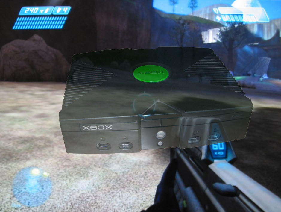
In 2001, Microsoft introduced its first game console, the Xbox. It was very close to a PC in terms of architecture. It used an x86 processor and ran Windows — and the graphics card was from Nvidia. The NV2A, as it was called, is an intermediate chip between the GeForce 3 and GeForce 4. It was well-optimized in the Xbox and supported DirectX 8.1 (through the console’s NT5 kernel), enabling the console to offer some very graphically impressive games for its time.
| Date released | November 2001 |
| Card interface | N/A |
| Fillrate | 1864 Mtexels/s |
| Fillrate | 932 Mpixels/s |
| Rendering pipelines | 4 |
| Texture units | 8 |
| Vertex units | 2 |
| Chip clock frequency | 233 MHz |
| Fabrication process | 0.15 µ |
| Number of transistors | 63 million |
| DirectX version | 8.1 |
| Memory Type | DDR |
| Maximum memory | 64 MB |
| Memory clock frequency | 200 MHz (x2) |
| Memory bus | 128 bits |
| Maximum bandwidth | 6.4 GB/s |
For the Xbox 360, ATI supplied the GPU and Nvidia went over to the enemy with its RSX chip used in the PlayStation 3.
An Improved GeForce 3: The GeForce 4 Ti
The successor to the GeForce 3, released in February 2002, was called the GeForce 4 Ti. Its architecture was similar to that of the NV20 (GeForce 3), but the NV25 was significantly faster due to its 150 nm process. Nvidia gave the GeForce 4 Ti approximately three times the Vertex Shader power of the GeForce 3 by increasing the clock frequency and doubling the number of ALUs. In addition, Nvidia improved LMA, the technology that limits memory bandwidth use by not calculating undisplayed data.
Nvidia sold three versions of the card: the Ti 4200, the Ti 4400 and the Ti 4600. The differences among the cards was in the clock speeds: 250 MHz for the GPU and 250 MHz for the memory (Ti 4200); 275/275 for the Ti 4400; and 300/325 for the high-end Ti 4600.
| Date released | February 2002 |
| Card interface | PCI/AGP 4x |
| Fillrate | 2400 Mtexels/s |
| Fillrate | 1200 Mpixels/s |
| Rendering pipelines | 4 |
| Texture units | 8 |
| Vertex Shader units | 2 |
| Version Shader | 1.3 |
| Chip clock frequency | 300 MHz |
| Fabrication process | 0.15 µ |
| Number of transistors | 63 million |
| DirectX version | 8 |
| Memory Type | DDR |
| Maximum memory | 128 MB |
| Memory clock frequency | 325 MHz (x2) |
| Memory bus | 128 bits |
| Maximum bandwidth | 10.4 GB/s |
| Video out | 2 x VGA |
| RAMDAC | 350 MHz |
| Video playback | MPEG2 semi-hardware |
Late in 2002, the NV28 arrived. This GPU was similar to the NV25, simply adding AGP 8x support to the GeForce 4 Ti cards. The GeForce Ti 4800 (300/325) was identical to the GeForce 4 Ti 4600 except for the addition of AGP 8x compatibility. The GeForce Ti 4200 128 MB had a lower bandwidth than the 64 MB version because the memory ran at 222 MHz compared to 250 MHz in the 64 MB version.
-
No way will nvidia release a 9800GT or 9800GTS as stated in the article, because there is already a 9800GTX, unless nvidia wants to kill themselves.Reply
-
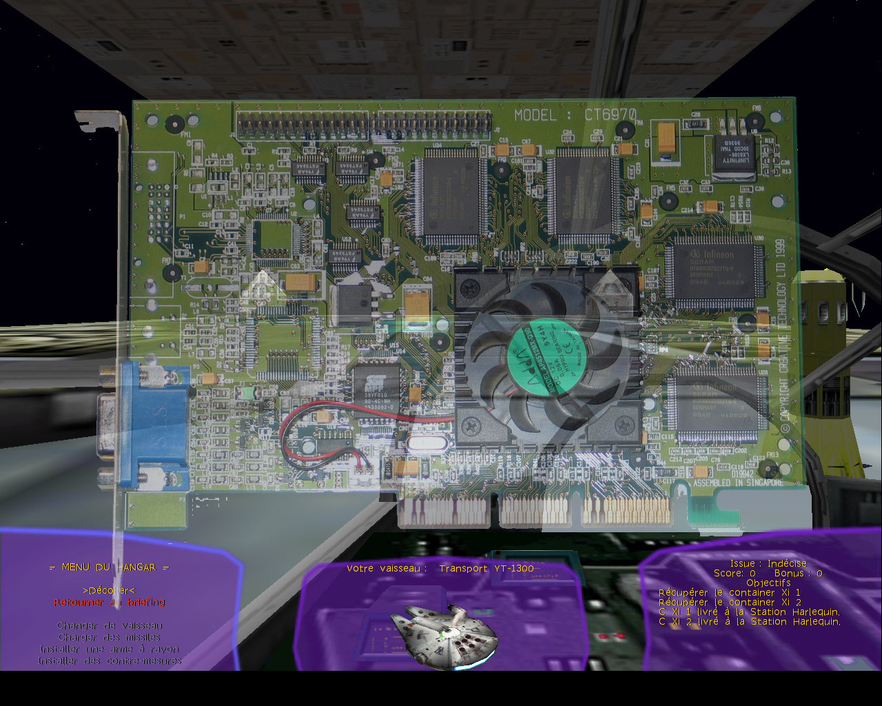
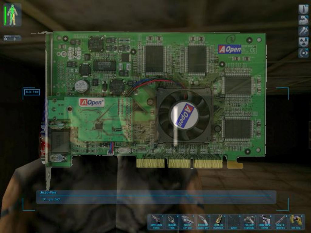
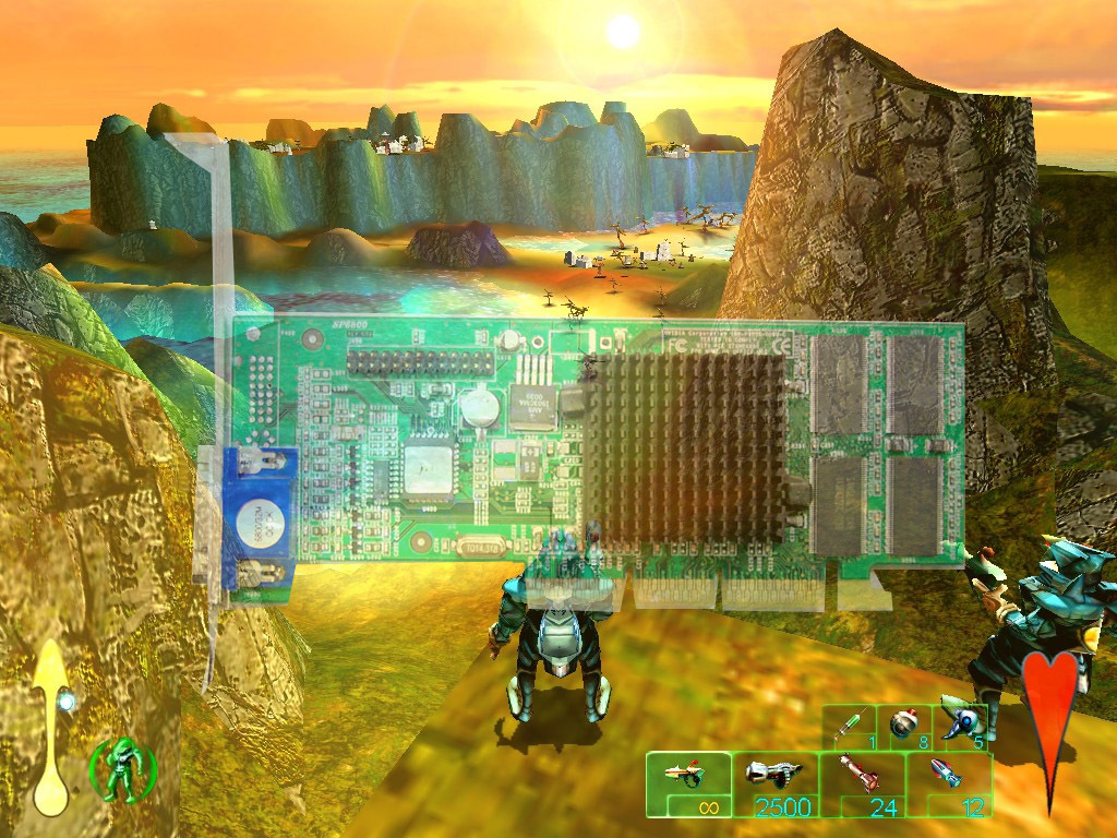
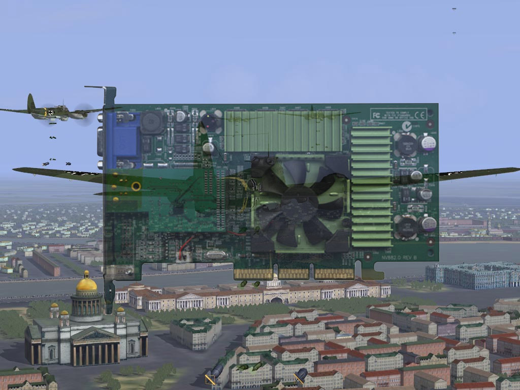
shmuls Here's a fun game for all the family: Can you name all the games pictured by their screenshot and year alone? I got 11 out of 19, can anyone name all 19? I'm sure lots of you can name the more recent ones, but how many hardcore gamers out there can get the earlier ones as well?!Reply
p.s. Great article, now lets see what Nvidia has in store for us in Q3/4!! -
giovanni86 Great article. I like how at the end the one selling the most is Intel. Good stuff.Reply -
radnor Not a bad article, but comes with a strange timing behind it. Is Nvidia selling THAT bad ?Reply
To make this a top of the line article, ya should include the Matrox Cards (Excelent in the early days), 3Dfx cards (V3000 and SLI V2 would still eat TNT2 in Image quality and performance), and last but not least (the sole survivor) ATI cards.
Now that would be a sight for sore eyes. -
dieseldre2k awesome trip down memory lane. thanks for the article. was wondering if could u make an ATI article also.Reply
and then maybe an AMD and Intel one too =P -
JonnyDough I would like to see the pictures organized in the order they are here in the slideshow. Also, could you perhaps rename them according to both card AND game so that when I scroll over them I can see what game it is? It would be of interest to me to research and consider purchase or download of an emulator of these old games.Reply
Thanks! -
hurbt My first thought when reading this article was that it's an obituary... lets review the history of Nvidia because ATI is kicking the crap out of them with their 4800 series... I know Nvidia isn't going anywhere, but that was just my first thought...Reply
I owned a TNT back when I first went to college. Descent 2 was so great on it, as was Total Annihilation. Half-life wasn't half bad on it either. It couldn't hold a candle to a couple Voodoo2's in SLI, though :) Too bad I had to return one of them, b/c I couldn't go without beer money. You gotta have your priorities straight in college, or you will get side-tracked... -
invlem My 3D evolution:Reply
Hercules 3d Prophet (2mb!!)
Diamond Voodoo 2 (8mb)
3DFX Voodoo 3 3000 (16mb)
ATi 7500 Pro (64mb)
ATi 9800 Pro (128mb)
eVGA 8800 GT (640mb)
