13 Years of Nvidia Graphics Cards
Get Tom's Hardware's best news and in-depth reviews, straight to your inbox.
You are now subscribed
Your newsletter sign-up was successful
NV30: Nvidia Loses With The FX 5800
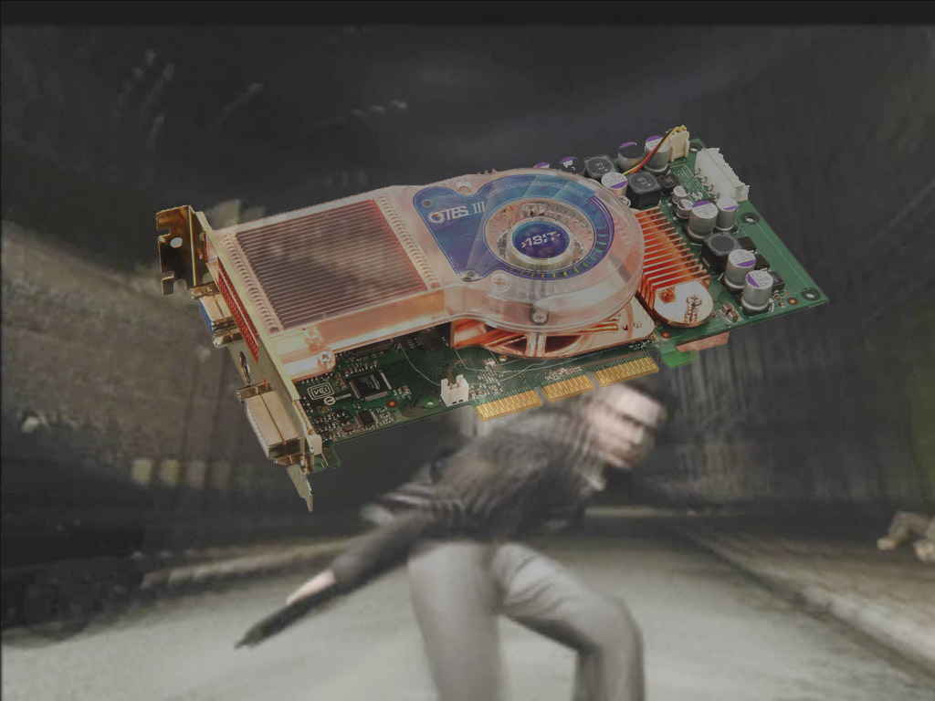
In January 2003, Nvidia released the GeForce FX 5800 (NV30). This card was criticized both for its performance, which was unworthy of a high-end card, and its high noise level. Released at around the same time, ATI’s Radeon 9700 Pro was much more efficient and also faster. The NV30 was a commercial failure, even if Nvidia sometimes says that the failure is one of the best things that have happened to the company — since it proved that you can never rest on your laurels.
| Date released | January 2003 |
| Card interface | PCI/AGP 8x |
| Fillrate (Mtexels) | 3200 Mtexels/s |
| Fillrate (Mpixels) | 1600 Mpixels/s |
| Rendering pipelines | 4 |
| Texture units | 8 |
| Vertex Shader units | 2 |
| Pixel Shader version | 2.0a |
| Chip clock frequency | 400 MHz |
| Fabrication process | 0.13 µ |
| Number of transistors | 125 million |
| DirectX version | 9 |
| Memory Type | DDR2 |
| Memory (generally) | 128 MB |
| Memory clock frequency | 400 MHz (x2) |
| Memory bus | 128 bits |
| Maximum bandwidth | 12.8 GB/s |
| Video out | 2 x VGA |
| RAMDAC | 400 MHz |
| Video playback | MPEG2 hardware |
The Ultra version of the card was faster (or shall we say less slow), with a clock speed of 500 MHz for the GPU and memory (DDR2).
NV3x: Nvidia Releases FX (and PCX) Versions
Even after the failure of the NV30, Nvidia kept the architecture, with the GeForce FX 5900 replacing the GeForce FX 5800. With its 256-bit memory bus and improved vertex calculating power, the FX 5900 managed to hold its own against competing cards like the Radeon 9800 Pro. Nvidia also released entry-level and midrange versions of its GeForce FX: the FX5600 (NV31) and FX5700 (NV36) in the midrange, and the entry-level FX5200 (NV34). These cards are noteworthy in that the earlier midrange card (the GeForce 4 Ti 4200) could outperform them.
| Name of the card | NV35 (FX 5900) | NV31 (FX 5600) | NV36 (FX 5700) | NV34 (FX 5200) |
| Date released | May 2003 | March 2003 | October 2003 | March 2003 |
| Card interface | PCI/AGP 8x | PCI/AGP 8x | PCI/AGP 8x | PCI/AGP 8x |
| Fillrate (Mtexels) | 3200 Mtexels/s | 1300 Mtexels/s | 1700 Mtexels/s | 1000 Mtexels/s |
| Fillrate (Mpixels) | 1600 Mpixels/s | 1300 Mpixels/s | 1700 Mpixels/s | 1000 Mpixels/s |
| Rendering pipelines | 4 | 4 | 4 | 4 |
| Texture units | 8 | 4 | 4 | 4 |
| Vertex Shader units | 3 | 1 | 3 | 1 |
| Chip clock frequency | 400 MHz | 325 MHz | 425 MHz | 250 MHz |
| Fabrication process | 0.13 µ | 0.13 µ | 0.13 µ | 0.13 µ |
| Number of transistors | 130 million | 80 million | 82 million | 47 million |
| DirectX version | 9 | 9 | 9 | 9 |
| Pixel Shader version | 2.0a | 2.0a | 2.0a | 2.0a |
| Memory Type | DDR | DDR | DDR | DDR |
| Memory (generally) | 256 MB | 128 MB | 256 MB | 128 MB |
| Memory clock frequency | 425 MHz (x2) | 275 MHz (x2) | 250 MHz (x2) | 200 MHz (x2) |
| Memory bus | 256 bits | 128 bits | 128 bits | 128 bits |
| Maximum bandwidth | 27.2 GB/s | 8.8 GB/s | 8 GB/s | 6.4 GB/s |
| Video out | 2 x VGA | 2 x VGA | 2 x VGA | 2 x VGA |
| RAMDAC | 400 MHz | 350 MHz | 350 MHz | 350 MHz |
| Video playback | MPEG2 hardware | MPEG2 hardware | MPEG2 hardware | MPEG2 hardware |
Nvidia also released PCI Express cards — the GeForce PCX series — but they were essentially AGP cards with an AGP-to-PCI Express bridge. Some FX 5200 cards had a 64-bit bus (instead of 128-bit) and a slower memory clock frequency (166 MHz instead of 200 MHz).
N40/N45: Nvidia Gets Back In The Race With The GeForce 6800 and SLI
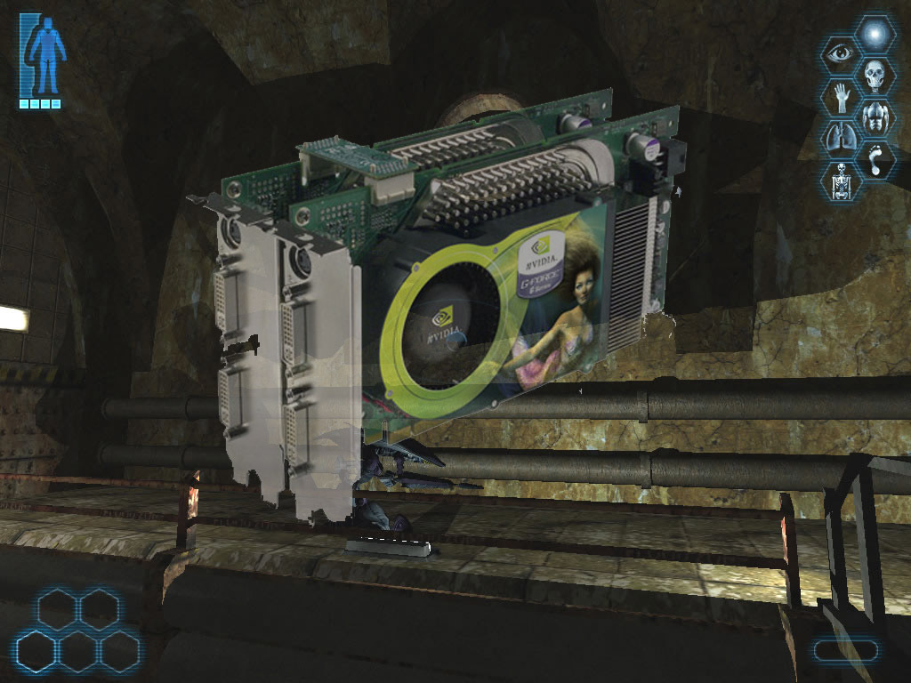
After the failure of the NV30, it was imperative of Nvidia to snap back. And they did, with the NV40, also known as the GeForce 6800. This card was extremely efficient and more powerful than the FX 5900, due to its large number of transistors (222 million). The NV45, also called GeForce 6800, was nothing more than an NV40 with an AGP-to-PCI Express bridge, giving the card support for the new standard, and above all, for SLI. The SLI technology couples two PCI Express GeForce 6 cards to increase performance.
| Date released | April 2004 | March 2005 |
| Card interface | AGP 8x | PCI Express 16x |
| Fillrate (Mtexels) | 6400 Mtexels/s | 6400 Mtexels/s |
| Fillrate (Mpixels) | 6400 Mpixels/s | 6400 Mpixels/s |
| Rendering pipelines | 16 | 16 |
| Texture units | 16 | 16 |
| Vertex Shader units | 6 | 6 |
| Chip clock frequency | 400 MHz | 400 MHz |
| Fabrication process | 0.13 µ | 0.13 µ |
| Number of transistors | 222 million | 222 million |
| DirectX version | 9c | 9c |
| Pixel Shader Version | 3.0 | 3.0 |
| Memory Type | GDDR3 | GDDR3 |
| Memory (generally) | 256 MB | 256 MB |
| Memory clock frequency | 550 MHz (x2) | 550 MHz (x2) |
| Memory bus | 256 bits | 256 bits |
| Maximum bandwidth | 35.2 GB/s | 35.2 GB/s |
| Video out | 2 x VGA | 2 x VGA |
| RAMDAC | 400 MHz | 400 MHz |
| Video playback | MPEG2 hardware | MPEG2 hardware |
| Multi-GPU support | N/A | 2 |
Cards based on the NV41 and NV42 were also produced. The NV41 is an NV40 with fewer processing units (12 pipelines and 5 vertex units) used in certain GeForce 6800 cards; the NV42 is an NV41 fabricated with a 110 nm process (and thus, less expensive to produce).
GeForce 6 Invades The Planet
After the GeForce 6800, Nvidia needed to introduce cards that were slower and less expensive. The NV40 was powerful, but its 222 million transistors limited fabrication yields and increased the price, so the two cards built from it, the GeForce 6600 and 6200, had only moderate success. The GeForce 6600, fabricated at 110 nm, was based on the NV43 and offered good performance at a decent price. The PCI Express versions of these cards could even operate in SLI mode.
The GeForce 6600 was the first natively PCI Express Nvidia card; AGP versions used a PCI Express-to-AGP bridge. The GeForce 6200 was an entry-level card — not very powerful but not very expensive. PCI Express, AGP, and PCI versions were produced, and there were also versions built into laptops.
Get Tom's Hardware's best news and in-depth reviews, straight to your inbox.
| Date released | August 2004 | August 2004 |
| Card interface | PCI Express 16x | PCI Express 16x |
| Fillrate (Mtexels) | 4000 Mtexels/s | 1400 Mtexels/s |
| Fillrate (Mpixels) | 2000 Mpixels/s | 700 Mpixels/s |
| Rendering pipelines | 4 | 2 |
| Texture units | 8 | 4 |
| Vertex shader units | 3 | 3 |
| Chip clock frequency | 500 MHz | 350 MHz |
| Fabrication process | 0.11 µ | 0.11 µ |
| Number of transistors | 143 million | 77 million |
| DirectX version | 9c | 9c |
| Pixel Shader version | 3.0 | 3.0 |
| Memory Type | GDDR3 | GDDR3 |
| Memory (generally) | 128 MB | 64 MB |
| Memory clock frequency | 450 MHz (x2) | 350 MHz (x2) |
| Memory bus | 128 bits | 64 bits |
| Maximum bandwidth | 14.2 GB/s | 5.6 GB/s |
| Video out | 2 x VGA | 2 x VGA |
| RAMDAC | 400 MHz | 400 MHz |
| Video playback | MPEG2 hardware | MPEG2 hardware |
| Multi-GPU support | 2 | N/A |
The GeForce 6200 was the first TurboCache card from Nvidia. In addition to the dedicated memory (16 to 512 MB), the card can use system RAM as video memory. Some manufacturers took advantage of this to tout the GeForce 6200 as “256 MB,” when in fact it had only 64 MB of dedicated memory. Note also that a built-in version of the NV44, the GeForce 6100, was included in certain Nvidia chipsets. The chip used a 90 nm process and had a single rendering pipeline and no dedicated memory.
G70 and G71: Nvidia Changes Its Nomenclature
In 2005, Nvidia announced the GeForce 7. The GPUs’ code name, which had traditionally been NVxx, changed to Gxx. The first card was the G70 (GeForce 7800), followed fairly quickly by the G71 (GeForce 7900). More powerful than the 6800 series, the GeForce 7800 was a success for Nvidia. The cards were sold in many different versions, such as the GTX and GS. AGP versions with a PCI Express-to-AGP bridge were also sold.
| Date released | June 2005 | March 2006 |
| Card interface | PCI Express 16x | PCI Express 16x |
| Fillrate (Mtexels) | 13200 Mtexels/s | 15600 Mtexels/s |
| Fillrate (Mpixels) | 8800 Mpixels/s | 10400 Mpixels/s |
| Rendering pipelines | 16 | 16 |
| Texture units | 24 | 24 |
| Vertex units | 8 | 8 |
| Chip clock frequency | 550 MHz | 650 MHz |
| Fabrication process | 0.11 µ | 0.09 µ |
| Number of transistors | 302 million | 278 million |
| DirectX version | 9c | 9c |
| Pixel Shader version | 3.0 | 3.0 |
| Memory Type | GDDR3 | GDDR3 |
| Memory (generally) | 512 MB | 512 MB |
| Memory clock frequency | 850 MHz (x2) | 800 MHz (x2) |
| Memory bus | 256 bits | 256 bits |
| Maximum bandwidth | 54.4 GB/s | 51.2 GB/s |
| Video out | 2 x VGA | 2 x VGA |
| RAMDAC | 400 MHz | 400 MHz |
| Video playback | MPEG2 hardware, WMV9 semi-hardware | MPEG2 hardware, WMV9 semi-hardware |
| Multi-GPU support | 2 | 4 (2x2) |
With the GeForce 7900 Nvidia also used, for the first time, a technique its competitors had already been using: dual-GPU cards. The 7900GX2 and 7950GX2 had two G71s in parallel. The company was to re-use this technique in 2008 with the GeForce 9800GX2.
G72 and G73: Low-end GeForce 7s
As has become its habit, Nvidia released two other versions of its high-end architecture — one entry-level (G72, GeForce 7300) and one midrange (G73, GeForce 7600). Both chips were fabricated with a 90 nm process and offered adequate performance. As is often the case, the mobile versions used the midrange chips, and the GeForce 7300 Go was very popular.
| Date released | January 2006 | March 2006 |
| Card interface | PCI Express 16x | PCI Express 16x |
| Fillrate (Mtexels) | 2200 Mtexels/s | 6720 Mtexels/s |
| Fillrate (Mpixels) | 1100 Mpixels/s | 4480 Mpixels/s |
| Rendering pipelines | 2 | 8 |
| Texture units | 4 | 12 |
| Vertex Shader units | 3 | 5 |
| Chip clock frequency | 550 MHz | 560 MHz |
| Fabrication process | 0.09 µ | 0.09 µ |
| Number of transistors | 112 million | 177 million |
| DirectX version | 9c | 9c |
| Pixel Shader version | 3.0 | 3.0 |
| Memory Type | GDDR | GDDR3 |
| Memory (generally) | 128 MB | 256 MB |
| Memory clock frequency | 400 MHz (x2) | 700 MHz (x2) |
| Memory bus | 64 bits | 128 bits |
| Maximum bandwidth | 6.4 GB/s | 22.4 GB/s |
| Video out | 2 x VGA | 2 x VGA + 2 x TDMS |
| RAMDAC | 400 MHz | 400 MHz |
| Video playback | MPEG2 hardware, WMV9 semi-hardware | MPEG2 hardware, WMV9 semi-hardware |
| Multi-GPU support | N/A | 2 |
Slower (7200 Go) and faster (7400 Go) portable versions were also produced, and an 80 nm version of the G73 was also sold by Nvidia.
Nvidia And The 8800: GeForce 8 Or GeForce 9?
In November 2006, Nvidia announced the G80. This chip and its derivatives were destined to have a long life. In fact, as of 2008, some of the fastest cards available from NVIDIA were still using a chip that’s very close to this G80 (the G92). Nvidia got as much mileage as possible out of the G80 and the move to a 65 nm process with the G92 allowed the company to save money on the cost of the chip. Nvidia varied the number of stream processors, the width of the memory bus, and clock speeds, in order to produce a plethora of GeForce 8800 and 9800 versions. There’s even a version with 2 GPUs: the GeForce 9800GX2.
The GeForce 8800 series cards were all DirectX 10 compatible, and Nvidia scored a great success with this series, pending the arrival of the GeForce GTX.
| Date released | November 2006 | April 2008 |
| Card interface | PCI Express 16x | PCI Express 16x (2.0) |
| Fillrate (Mtexels) | 18400 Mtexels/s | 43875 Mtexels/s |
| Fillrate (Mpixels) | 13800 Mpixels/s | 10800 Mpixels/s |
| Rendering pipelines | 24 | 16 |
| Texture units | 32 | 64 |
| Stream Processors | 128 | 128 |
| Chip clock frequency | 575 MHz | 675 MHz |
| Fabrication process | 0.09 µ | 0.065 µ |
| Number of transistors | 681 million | 754 million |
| DirectX version | 10 | 10 |
| Pixel Shader version | 4.0 | 4.0 |
| Memory Type | GDDR3 | GDDR3 |
| Memory (generally) | 768 MB | 512 MB |
| Memory clock frequency | 900 MHz (x2) | 1100 MHz (x2) |
| Memory bus | 384 bits | 256 bits |
| Maximum bandwidth | 86.4 GB/s | 70.4 GB/s |
| Video out | NVIO | 2 x TDMS (DualLink), HDCP |
| RAMDAC | 400 MHz | 400 MHz |
| Video playback | MPEG2 hardware, WMV9 semi-hardware | MPEG2 hardware, H.264 hardware |
| Multi-GPU support | 3 | 3 |
Just for a laugh, let’s run through all the GeForce 8800 series cards that have been released: the 8800GS 374, 8800GS 768, 8800GTS 320, 8800GTS 640, 8800GTS 640 v2, 8800GTS 512, 8800GT 256, 8800GT 512, 8800GT 1024, 8800GTX 768 and 8800 Ultra 768. Then there’s the 9600GSO 512, 9600GSO 384 and 9600GSO 768, and the 9800GX2 and 9800GTX — not to mention the future 9800GTS and 9800GT. And that’s not counting the mobile versions!
Entry-Level GeForce 8s
To be able to market economy versions of the card, Nvidia had to severely modify the G80. Given the number of transistors, it was out of the question to use it as-is. So the company offered three chips, more or less: the GeForce 8400 (G86), GeForce 8600 (G84) and GeForce 9600 (G94). Other versions existed (GeForce 8300, 8500, and so on), but those three models are the major ones. The G84 was much used in notebooks, as a high-end card, whereas in desktop PCs it was only a midrange GPU.
| Date released | April 2007 | June 2007 | February 2008 |
| Card interface | PCI Express 16x | PCI Express 16x | PCI Express 16x (2.0) |
| Fillrate (Mtexels) | 3600 Mtexels/s | 8640 Mtexels/s | 20800 Mtexels/s |
| Fillrate (Mpixels) | 1800 Mpixels/s | 4320 Mpixels/s | 10400 Mpixels/s |
| Rendering pipelines | 4 | 8 | 16 |
| Texture units | 8 | 16 | 32 |
| Stream Processors | 16 | 32 | 64 |
| Chip clock frequency | 450 MHz | 540 MHz | 650 MHz |
| Fabrication process | 0.08 µ | 0.08 µ | 0.065 µ |
| Number of transistors | 210 million | 289 million | 505 million |
| DirectX version | 10 | 10 | 10 |
| Pixel shader version | 4.0 | 4.0 | 4.0 |
| Memory Type | DDR2 | GDDR3 | GDDR3 |
| Memory (generally) | 256 MB | 256 MB | 512 MB |
| Memory clock frequency | 400 MHz (x2) | 700 MHz (x2) | 900 MHz (x2) |
| Memory bus | 64 bits | 128 bits | 256 bits |
| Maximum bandwidth | 6.4 GB/s | 22.4 GB/s | 57.6 GB/s |
| Video out | 2 x TDMS (DualLink), HDCP | 2 x TDMS (DualLink), HDCP | 2 x TDMS (DualLink), HDCP |
| RAMDAC | 400 MHz | 400 MHz | 400 MHz |
| Video playback | MPEG2 hardware, H.264 hardware | MPEG2 hardware, H.264 hardware | MPEG2 hardware, H.264 hardware |
| Multi-GPU support | N/A | 2 | 2 |
The GeForce 8600 and GeForce 8400 were as mediocre as the G80 and GeForce 8800 were successful. The spread between high-end and midrange cards (before the arrival of the GeForce 9600) is very wide for this generation, which causes problems for gamers.
Nvidia introduced its current GPU in June. It’s based on the G80 and improves on its performance and architecture (512-bit bus, 240 stream processors, etc.) You can read our review of the new top-of-the line GeForce GTX 280 and 260 here.
In conclusion, this article should have shown you that it hasn’t been all successes for Nvidia along the way, and that the company didn’t have an easy time of it in the early days. But it also shows how two companies have managed to do away with most of the competition in the field of graphics cards for gamers. Still, remember that the company that sells the most graphics solutions for PC is neither Nvidia nor AMD/ATI, but Intel.
We intentionally left out the characteristics of professional graphics cards (Quadro) and mobile versions. The former were omitted because the differences have to do mostly with prices and drivers, and the latter because Nvidia’s clock speeds for portable models are only recommendations, which means that there can be huge differences between two cards with the same name.
-
No way will nvidia release a 9800GT or 9800GTS as stated in the article, because there is already a 9800GTX, unless nvidia wants to kill themselves.Reply
-
shmuls Here's a fun game for all the family: Can you name all the games pictured by their screenshot and year alone? I got 11 out of 19, can anyone name all 19? I'm sure lots of you can name the more recent ones, but how many hardcore gamers out there can get the earlier ones as well?!Reply
p.s. Great article, now lets see what Nvidia has in store for us in Q3/4!! -
giovanni86 Great article. I like how at the end the one selling the most is Intel. Good stuff.Reply -
radnor Not a bad article, but comes with a strange timing behind it. Is Nvidia selling THAT bad ?Reply
To make this a top of the line article, ya should include the Matrox Cards (Excelent in the early days), 3Dfx cards (V3000 and SLI V2 would still eat TNT2 in Image quality and performance), and last but not least (the sole survivor) ATI cards.
Now that would be a sight for sore eyes. -
dieseldre2k awesome trip down memory lane. thanks for the article. was wondering if could u make an ATI article also.Reply
and then maybe an AMD and Intel one too =P -
JonnyDough I would like to see the pictures organized in the order they are here in the slideshow. Also, could you perhaps rename them according to both card AND game so that when I scroll over them I can see what game it is? It would be of interest to me to research and consider purchase or download of an emulator of these old games.Reply
Thanks! -
hurbt My first thought when reading this article was that it's an obituary... lets review the history of Nvidia because ATI is kicking the crap out of them with their 4800 series... I know Nvidia isn't going anywhere, but that was just my first thought...Reply
I owned a TNT back when I first went to college. Descent 2 was so great on it, as was Total Annihilation. Half-life wasn't half bad on it either. It couldn't hold a candle to a couple Voodoo2's in SLI, though :) Too bad I had to return one of them, b/c I couldn't go without beer money. You gotta have your priorities straight in college, or you will get side-tracked... -
invlem My 3D evolution:Reply
Hercules 3d Prophet (2mb!!)
Diamond Voodoo 2 (8mb)
3DFX Voodoo 3 3000 (16mb)
ATi 7500 Pro (64mb)
ATi 9800 Pro (128mb)
eVGA 8800 GT (640mb)
