Nvidia GeForce GTX 260/280 Review

Get Tom's Hardware's best news and in-depth reviews, straight to your inbox.
You are now subscribed
Your newsletter sign-up was successful
Introduction
Over a year and a half – that’s how long the GeForce 8800 GTX remained in the position of what could be called Nvidia’s high-end GPU. Oh of course, six months after its release and – just a coincidence – just before the arrival of the R600, we did get an 8800 Ultra with slightly higher clock speeds, but it was nothing revolutionary. Then two and a half months ago, the arrival of the 9800GTX awakened hopes of substantial performance increases, but in the end the card offered only limited gains over the good old GTX, and was behind the Ultra version. For owners of these cards to be really happy with their investment, it was high time for Nvidia to offer more than a few extra megahertz or to rely on pairing two GPUs on the same card.
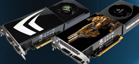
Finally Nvidia has heard our pleas: The GTX 280 is the first real reworking of the G8x architecture. And, yes, breaking with tradition, "GTX" is a prefix for this new architecture. Now we know the company’s modus operandi: Introduce a new architecture on a proven engraving process. Due to the often very high number of transistors, the chip is expensive to produce and the cards that use it remain expensive, but it stakes out the territory. Then during the ensuing years, Nvidia develops its architecture on all segments of the scale, using finer engraving, but it is less optimized for high clock speeds. Finally, when the new process is under control, Nvidia moves it into the high end, which then becomes much more affordable. We saw it with the G70/G71 and the G80/G92, and now history repeats itself with the GT200 – a true killer with 1.4 billion transistors engraved at 0.65 µm.
See our video of the GTX 280 (running) and the GTX 260 (shown).
Get Tom's Hardware's best news and in-depth reviews, straight to your inbox.
-
Lunarion what a POS, the 9800gx2 is $150+ cheaper and performs just about the same. Let's hope the new ATI cards coming actually make a differenceReply -
foxhound009 woow,.... that's the new "high end" gpu????Reply
lolz.. 3870 x2 wil get cheaper... and nvidia gtx200 lies on the shelves providing space for dust........
(I really expectede mmore from this one... :/ ) -
thatguy2001 Pretty disappointing. And here I was thinking that the gtx 280 was supposed to put the 9800gx2 to shame. Not too good.Reply -
cappster Both cards are priced out of my price range. Mainstream decently priced cards sell better than the extreme high priced cards. I think Nvidia is going to lose this round of "next gen" cards and price to performance ratio to ATI. I am a fan of whichever company will provide a nice performing card at a decent price (sub 300 dollars).Reply -
njalterio Very disappointing, and I had to laugh when they compared the prices for the GTX 260 and the GTX 280, $450 and $600, calling the GTX 260 "nearly half the price" of the GTX 280. Way to fail at math. lol.Reply -
NarwhaleAu It is going to get owned by the 4870x2. In some cases the 3870x2 was quicker - not many, but we are talking 640 shaders total vs. 1600 total for the 4870x2.Reply -
MooseMuffin Loud, power hungry, expensive and not a huge performance improvement. Nice job nvidia.Reply -
compy386 This should be great news for AMD. The 4870 is rumored to come in at 40% above the 9800GTX so that would put it at about the 260GTX range. At $300 it would be a much better value. Plus AMD was expecting to price it in the $200s so even if it hits low, AMD can lower the price and make some money.Reply -
vochtige i think i'll get a 8800ultra. i'll be safe for the next 5 generations of nvidia! try harder nv crewReply
