The History of Nvidia GPUs: NV1 to Turing
NV35: The FX 5000 Series (Part 2)
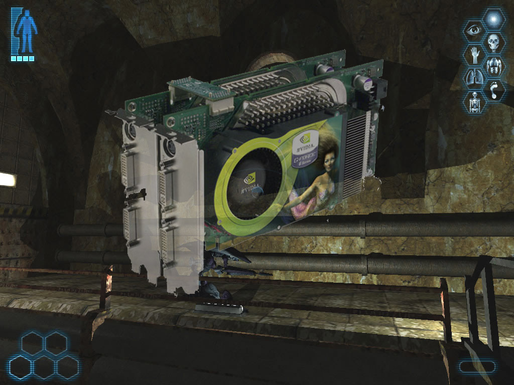
Although the NV30 was the original FX 5000-series flagship, just a few months later Nvidia released a faster model that had an extra vertex shader and could use DDR3 connected via a wider 256-bit bus.
The FX 5000 series was heavily criticized despite its advanced feature set because its lackluster performance lagged behind ATI's competing GPUs. It also had poor thermal characteristics, causing the GPU to run extraordinarily hot, requiring OEMs to sell the FX 5000 series with large air coolers.
NV40: Nvidia GeForce 6800
Just one year after the launch of the FX 5000 series, Nvidia released the 6000 series. The GeForce 6800 Ultra was Nvidia's flagship powered by the NV40. With 222 million transistors, 16 pixel superscalar pipelines (with one pixel shader, TMU, and ROP on each), six vertex shaders, Pixel Shader 3.0 support, and 32-bit floating-point precision, the NV40 had vastly more resources at its disposal than the NV30. This is also not counting native support for up to 512MB of GDDR3 over a 256-bit bus, giving the GPU more memory and better memory performance than its predecessor. These GPUs were produced with the same 130nm technology as the FX 5000 series.
The 6000 series was highly successful, as it could be twice as fast as the FX 5950 Ultra in some games, and was often roughly 50% faster in most tests. At the same time, it was also more energy efficient.
NV43: The GeForce 6600
After Nvidia secured its position at the high-end of the GPU market, it turned its attention to producing a new mid-range graphics chip known as the NV43. This GPU was used inside of the Nvidia GeForce 6600, and it had essentially half of the execution resources of the NV40. It also relied on a narrower 128-bit bus. The NV43 had one key advantage, however, as it was shrunk using 110 nm transistors. The reduced number of resources made the NV43 relatively inexpensive to produce, while he new fabrication technology helped reduce power consumption and boost clock speeds by roughly 20% compared to the GeForce 6600.
G70: The GeForce 7800 GTX And GeForce 7800 GTX 512
The GeForce 6800 was succeeded by the GeForce 7800 GTX, which used a new GPU code-named G70. Based on the same 110 nm technology as NV43, the G70 contained a total of 24 pixel pipelines with 24 TMUs, eight vertex shaders, and 16 ROPs. The GPU could access to up to 256MB of GDDR3 clocked at up to 600 MHz (1.2 GHz DDR) over a 256-bit bus. The core itself operated at 430 MHz.
Although the GeForce 7800 GTX was quite powerful for its time, Nvidia managed to improve upon its design shortly after its release with the GeForce 7800 GTX 512. With this card, Nvidia reworked the layout of the core and transitioned over to a new cooler design, which enabled the company to push clock speed up to 550 MHz. It also improved its memory controller by reducing latency, increasing the bus width to 512-bit, and pushing the memory frequency up to 850 MHz (1.7 GHz DDR). Memory capacity increased to 512MB, too.
Get Tom's Hardware's best news and in-depth reviews, straight to your inbox.
G80: GeForce 8000 Series And The Birth Of Tesla
Nvidia introduced its Tesla microarchitecture with the GeForce 8000 series - the company's first unified shader design. Tesla would become one of Nvidia's longest-running architectures, as it was used inside the GeForce 8000, GeForce 9000, GeForce 100, GeForce 200, and GeForce 300 series of GPUs.
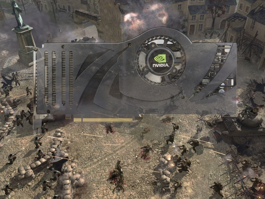
The GeForce 8000 series's flagship was the 8800 GTX, powered by Nvidia's G80 GPU manufactured at 80 nm with over 681 million transistors. Thanks to the unified shader architecture, the 8800 GTX and the rest of the 8000 series featured full support for Microsoft's new DirectX 10 API and Pixel Shader 4.0. The 8800 GTX came with 128 shaders clocked at 575 MHz and connected to 768MB of GDDR3 over a 384-bit bus. Nvidia also increased the number of TMUs up to 64 and raised the ROP count to 24. All of these enhancements allowed the GeForce 8800 GTX perform more than twice as fast as its predecessor in high-resolution tests.
As yields improved, Nvidia later replaced the 8800 GTX with the 8800 Ultra as the flagship. Although both graphics cards used the same G80 core, the 8800 Ultra was clocked at 612 MHz, giving it a slight edge over the 8800 GTX.
G92: GeForce 9000 Series And Tesla Improved
Nvidia continued to use the Tesla architecture in its GeForce 9000 series products, but with a few revisions. Nvidia's G92 core inside the 9000-series flagship was essentially just a die shrink of G80. By fabricating G92 at 65 nm, Nvidia was able to hit clock speeds ranging from 600 to 675 MHz all while reducing overall power consumption.
Thanks to the improved energy efficiency and reduced heat, Nvidia launched a dual-G92 GPU called the GeForce 9800 GX2 as the flagship in the 9000 series. This was something Nvidia was unable to do with the power-hungry G80. In tests, the 9800 GX2 outperformed the 8800 Ultra on average between 29 to 41% when AA was turned off. When AA was active, however, the 9800 GX2's performance lead shrunk to 13% due to RAM limitations. Each G92 on the 9800 GX2 had access to 512MB of GDDR3, while the 8800 Ultra came with 768MB. The card was also considerably more expensive than the 8800 Ultra, which made it a tough sale.
G92 And G92B: GeForce 9000 Series (Continued)
Nvidia later released the GeForce 9800 GTX with a single G92 core clocked at 675 MHz and 512MB of GDDR3. This 9800 GTX was slightly faster than the 8800 Ultra thanks to its higher clock speed, but it also ran into issues due to its limited RAM capacity. Eventually, Nvidia created the GeForce 9800 GTX+ with a new 55 nm chip code-named G92B. This allowed Nvidia to push clock speed up to 738 MHz, but the most significant improvement that the 9800 GTX+ possessed was its 1GB of memory.
G92B: The GeForce 100 Series
Towards the end of the 9000-series, Nvidia introduced the GeForce 100 series targeted exclusively at OEMs. Individual consumers were not able to buy any of the 100-series cards directly from retailers. All 100 series GPUs were re-branded variants of the 9000 series with minor alternations to clock speed and card design.
GT200: GeForce 200 Series And Tesla 2.0
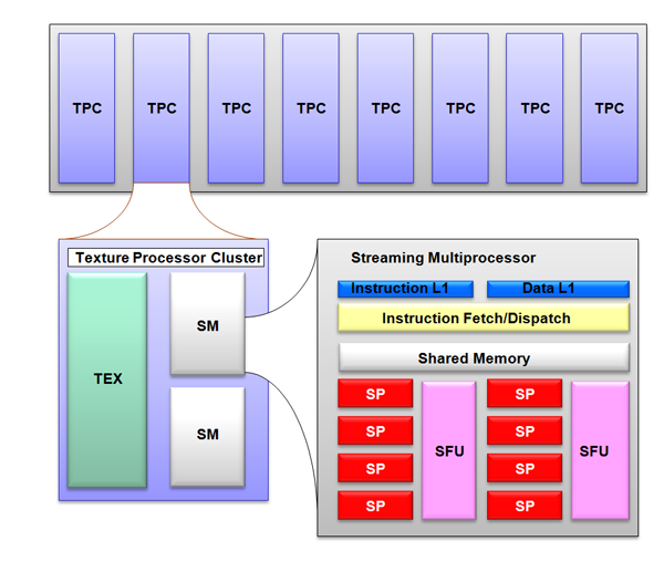
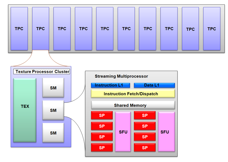
Nvidia introduced the GT200 core based on an improved Tesla architecture in 2008. Changes made to the architecture included an improved scheduler and instruction set, a wider memory interface, and an altered core ratio. Whereas the G92 had eight Texture Processor Clusters (TPC) with 16 EUs and eight TMUs, the GT200 used ten TPCs with 24 EUs and eight TMUs each. Nvidia also doubled the number of ROPs from 16 in the G92 to 32 in the GT200. The memory bus was extended from a 256-bit interface to a 512-bit wide connection to the GDDR3 memory pool.
The GT200 launched in the Nvidia GeForce GTX 280, which was significantly faster than the GeForce 9800 GTX+ due to the increased resources. It could not cleanly outperform the GeForce 9800 GX2, but because the 9800 GX2 had considerably higher power consumption and less memory, the GTX 280 was still considered the superior graphics card. The introduction of the GeForce GTX 295 with two GT200 cores in 2009 further cemented the market position of the 200 series.
MORE: Gaming At 3840x2160: Is Your PC Ready For A 4K Display
GT215: The GeForce 300 Series
The GeForce 300 series was Nvidia's second OEM-only line of cards. It was composed entirely of medium-range and low-end GPUs from the GeForce 200 series. All GeForce 300 series desktop GPUs use a 40 nm process and are based on the Tesla 2.0 architecture.
-
abryant Archived comments are found here: http://www.tomshardware.com/forum/id-3407581/history-nvidia-gpus.htmlReply -
kinggremlin So, based on the archived comments, this is the THIRD time this article has been posted since the release of Pascal. Why on earth would you keep recycling this article when nothing has been added to the "history?" Turing has not been released yet, we have no benchmarks. Unless this site has no intention of posting reviews of the Turing cards, there is zero reason to re-re-post this just to add an unreleased architecture on the last slide with no useful or new information.Reply -
bit_user Anyone interested in early GPUs (particularly Nvidia's exotic NV1 and its cancelled successor) would probably find this a worthwhile read:Reply
http://vintage3d.org/nv1.php#sthash.AWlq2ihY.dpbs
He thoroughly explores their unique quadric rendering approach, including its down-sides and how they tried to mitigate.
The author of that site has posted on here, in a previous article about vintage 3D cards. Maybe he'll show up, again. -
Blytz I really love to see a graph of the processing power and memory bandwidth of the evolution of these cards (and throw in the ati/radeons as well) to see when we made leaps or increments and how far it's all come.Reply -
bit_user Reply
This isn't exactly relevant to graphics performance, but still worth a look.21265764 said:I really love to see a graph of the processing power and memory bandwidth of the evolution of these cards (and throw in the ati/radeons as well) to see when we made leaps or increments and how far it's all come.
https://www.karlrupp.net/2013/06/cpu-gpu-and-mic-hardware-characteristics-over-time/
Note that the Y-axis of most plots is in log-scale. Also, even though it's from 2013, he updated it for KNL and Pascal. I just wish he'd update it with Volta.
Edit: If you liked that, you might enjoy his 42 Years of Microprocessor Trend Data. -
Unsal Ersoz Wow, I was a very hardcore gamer back then :)Reply
TNT2 and Voodoo3 were competitors until 3DFX released its January 2000 drivers. I can remember it like yesterday. That miniGL port for the opengl games like half-life, quake and others that is long forgotten basically blew tnt2 to the dust (I owned both of the hardware). At 2000, Nvidia was very incompetitive from the software perspective compared to 3dfx with voodoo3. I remember my GLquake renders 10720fps timelapse while tnt2 was stuck with ~60ish :)
Nice memories. -
samopa I am in 3dfx camp until I had forced to switch to nVidia camp. I owned Voodoo1, Banshee, Voodoo2, Voodoo3 3000, Voodoo5 5500 before finally switch to GeForce 6800 Ultra.Reply
Such a fond memories -
AgentLozen I remember posting a comment on this article the last time it came around.Reply
I mentioned last time that I liked the video game screenshots in the background. It helps put the hardware into perspective. For example, the TNT was meant to play games like Half Life. The TNT2 was built to take on Quake 3.
My unique contribution this time is that I would like to see the date of each card's release on each slide. Some entries have this and others don't. I mentioned perspective in my last paragraph and the same applies here. A good analogy for why the date is important would be like taking a history class and hearing "In 1941, America entered World War 2. A short time later, America found itself in Vietnam." So...... was America in Vietnam in that same decade? In the 1950's? The 1960's? It would help my understanding to have a date.
I did enjoy reading this article even if I've looked at it before. -
Stephen_144 The 3dfx was my second gfx card. My second computer, a Pentium 90, had a Diamond Viper Stealth card which I later upgraded to a 3DFX.Reply
I recall loading Windows for Work groups because I could get a 800x600 resolution all the way up to 256 colors. That was up from 640x480 16 colors in the regular windows 3.0. I recall being amazing all the images and spent the entire day downloading (from my dial up Comp-u-Serve 28k modem) color icons and customizing all my windows to use them. Awww simpler times. -
steve.d.moss Is this another biased article like the one telling us to buy RTX cards without even waiting for concrete proof of performance and at inflated prices? I really hope not.Reply
The history of Nvidias rise to power is far more convoluted and full of lies, skullduggery and deceit than people realise.
Check out Adored TV on YouTube. He did a totally unbiased and crystal clear video on this topic a few months back.
Definitely worth a watch, might even open your eye a little.

