The History of Nvidia GPUs: NV1 to Turing
GF100: Fermi Arrises In The GeForce 400
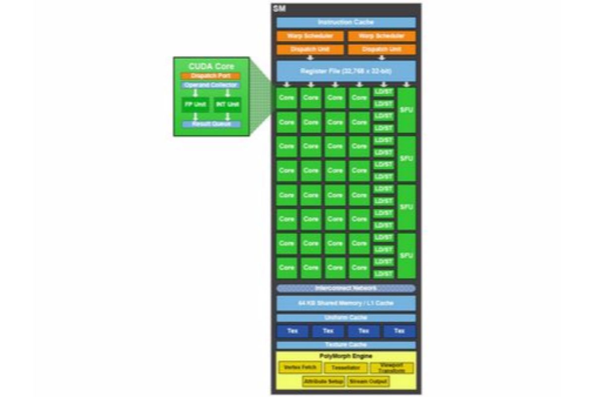
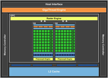
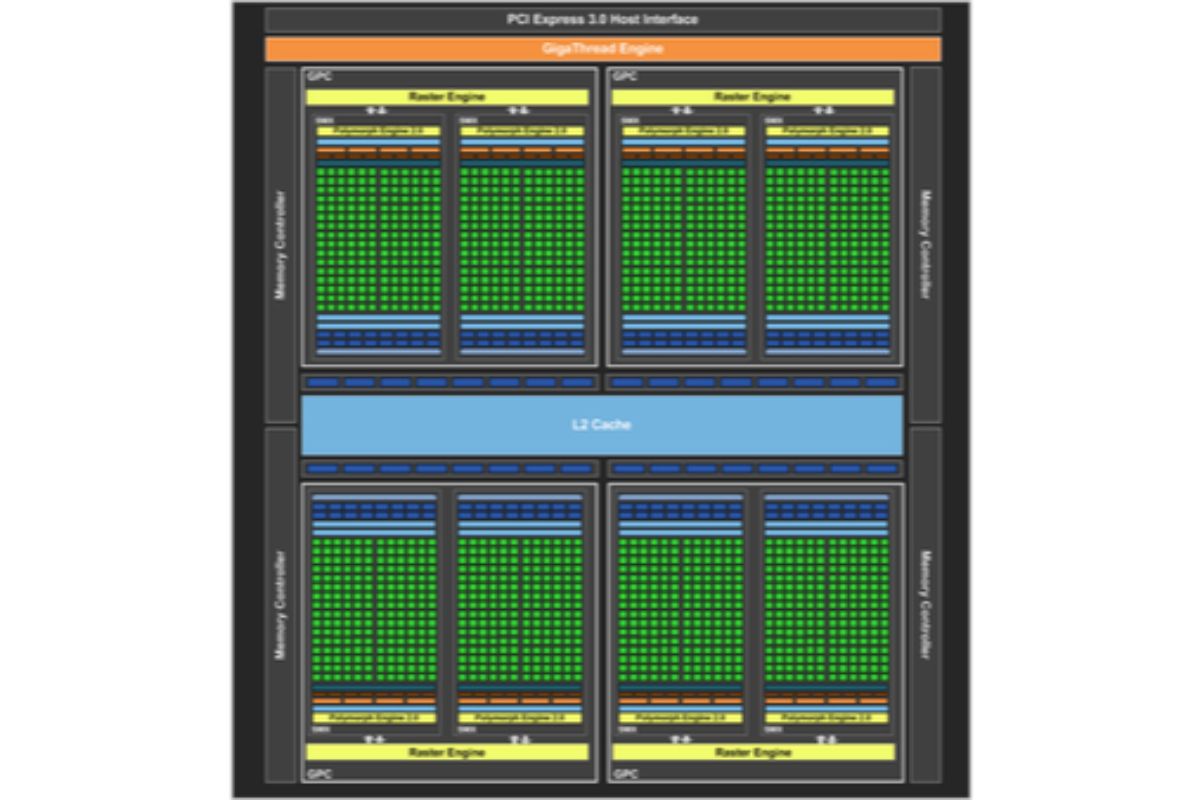
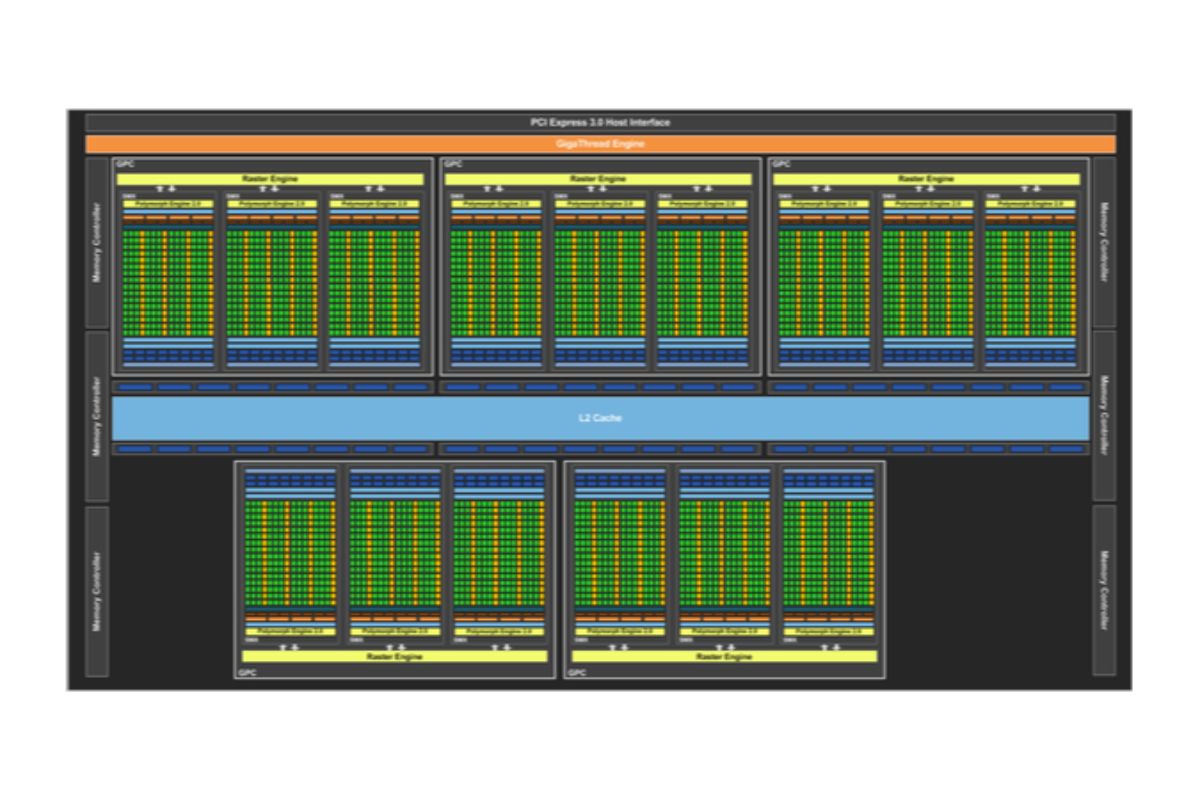
Tesla and the GeForce 8000, 9000, 100, 200, and 300 series were followed by Nvidia's Fermi architecture and the GeForce 400 series in 2010. The largest Fermi chip ever produced was the GF100, which contained four GPCs. Each GPC had four Streaming Multiprocessors, with 32 CUDA cores, four TMUs, three ROPs, and a PolyMorph Engine. A perfect GF100 core shipped with a total of 512 CUDA cores, 64 TMUs, 48 ROPs, and 16 PolyMorph Engines.
However, the GeForce GTX 480 ( the original Fermi flagship) shipped with just 480 CUDA cores, 60 TMUs, 48 ROPs, and 15 PolyMorph Engines enabled. Due to the hardware resources present in GF100, it was an enormous 529 square millimeters in area. This made it rather difficult to produce perfect samples, and forced Nvidia to use slightly defective cores instead. The GeForce GTX 480 also gained a reputation for running excessively hot. Nvidia and its board partners typically used beefy thermal solutions on the GTX 480 as well, which tended to be loud and earned the graphics card a reputation as one of the nosiest GPUs in recent years.
GF104, 106, 108: Fermi's Alterted Cores
To reduce production costs and increase yields of its smaller Fermi GPUs, Nvidia rearranged the resource count of its SMs. Each of the eight SMs inside the GF104 and four inside the GF106 contain 48 CUDA cores, four TMUs, and four ROPs. This reduced the overall die size, as less SMs were needed on each die. It also reduced shader performance somewhat, but these cores were nonetheless competitive. With this core configuration, an Nvidia GeForce GTX 460 powered by a GF104 was able to perform nearly identical to an Nvidia GeForce GTX 465 that contained a GF100 core with just 11 SMs enabled.
When Nvidia created the GF108, it again altered the number of resources in each SM. The GF108 has just two SMs, which contain 48 CUDA cores, four TMUs, and two ROPs each.
GF110: Fermi Re-Worked
Nvidia continued to use the Fermi architecture for the GeForce 500 series, but managed to improve upon its design by re-working each GPU on a transistor level. The underlying concept of this re-working process was to use slower more efficient transistors in some parts of the GPU that are less critical to performance, and to use faster transistors in key areas that strongly affect performance. This had the impact of reducing power consumption and enabling an increase in clock speed.
Under the hood of the GTX 580 (the GeForce 500-series flagship) was GF110. In addition to the aforementioned transistor re-working, Nvidia also improved FP16 and Z-cull efficiency. These changes made it possible to enable all 16 SMs on the GF110, and the GTX 580 was considerably faster than the GTX 480.
GK104: Kepler And The 600 Series
The GeForce GTX 580 was succeeded by the GTX 680, which used a GK104 based on the Kepler architecture. This marked a transition to 28 nm manufacturing, which is partially responsible for the GK104 being far more efficient than GF110. Compared to the GF110, GK104 also has twice as many TMUs and three times as many CUDA cores. The increase in resources didn't triple performance, but it did increase performance by between 10 and 30% depending on the game. Overall efficiency increased even more.
Get Tom's Hardware's best news and in-depth reviews, straight to your inbox.
GK110: Big Kepler
Nvidia's plan for the GeForce 700 series was essentially to introduce a larger Kepler die. The GK110, which was developed for compute work inside of supercomputers, was perfect for the job. This massive GPU contained 2880 CUDA cores and 240 TMUs. It was first introduced inside the GTX Titan, which had a single SMX disabled, dropping the core count to 2688 CUDA cores, 224 TMUs, and 6GB of RAM. However, the Titan had an unusually high price of $1000, which limited sales. It was later re-introduced as the GTX 780 with just 3GB of RAM and a somewhat more affordable price tag.
Later, Nvidia would ship the GTX 780 Ti, which fully utilized the GK110 with all 2880 CUDA cores and 240 TMUs.
GM204: Maxwell
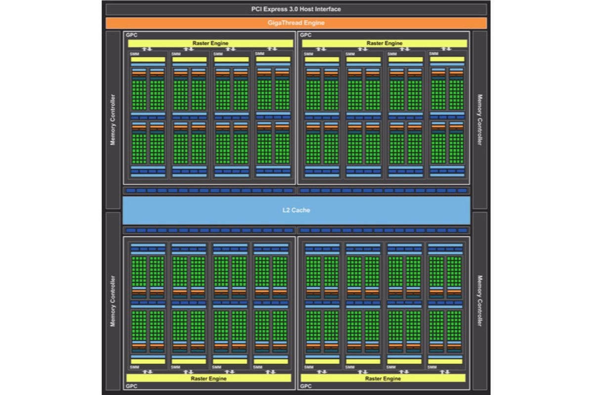
Nvidia introduced its Maxwell architecture in 2014 with a focus on efficiency. The initial flagship, the GM204, launched inside the GeForce GTX 980. A key difference between Maxwell and Kepler is the memory sub-system. GM204 has a narrower 256-bit bus, but Nvidia achieved greater utilization of the available bandwidth by implementing a powerful memory compression algorithm. The GM204 also utilizes a large 2MB L2 cache that further reduced the impact of the narrower memory interface.
The GM204 contained a total of 2048 CUDA cores, 128 TMUs, 64 ROPs, and 16 PolyMorph engines. Due to the reduced resources compared to the GTX 780 Ti, the GM204 wasn't exceptionally faster than the GeForce GTX 780 Ti. It achieved just a 6% performance advantage over the GTX 780 Ti, but it also consumed roughly 33% less power.
Nvidia later released the GM200 inside the GeForce GTX 980 Ti. The GM200 was essentially a more resource-rich GM204 with 2816 CUDA cores. It managed to increase performance over the GM204, but it was not quite as efficient.
GP104: Pascal
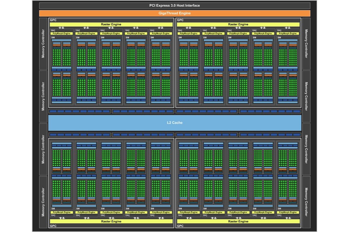
The Pascal architecture succeeded Maxwell, and marked Nvidia's transition to a new 16 nm FinFET process. This helped to increase the architectural efficiency and drive up clock speed. The 314 mm square GP104 used inside the GeForce GTX 1080 contains a whopping 7.2 billion transistors. With 2560 CUDA cores, 160 TMUs, 64 ROPs, and 20 PolyMorph engines, the GeForce GTX 1080 was far more powerful than the GeForce GTX 980 Ti.
Nvidia also produced four other GPUs based on Pascal with lower core counts. Like the GTX 1080, the GTX 1070 is targeted at the high-end gaming segment, while the GTX 1060 handles the mid-range segment, and the GeForce GTX 1050 and 1050 Ti handle the low-end of the market.
GP102: Titan X, 1080 Ti & Titan XP
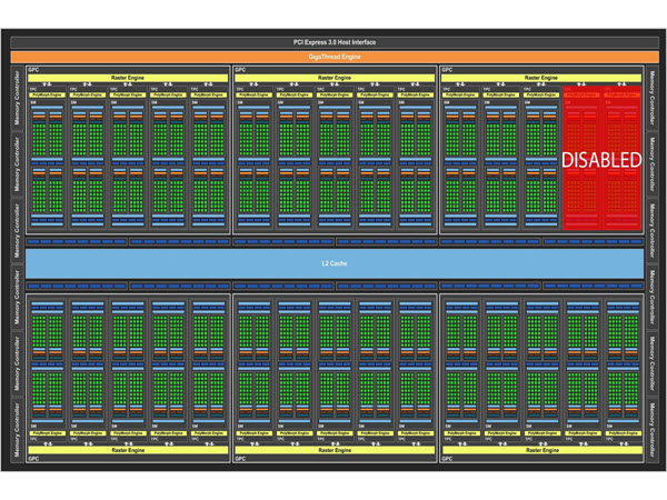
Nvidia pushed the performance of the 1000 series further with the release of its GP102 GPU. This part features 3,840 CUDA cores with a 352-bit memory interface, and it is also produced on a 16nm process. It first appeared inside of the Titan X with a partially disabled die that left 3,584 cores clocked at 1,531MHz. It was equipped with 12GB of GDDR5X memory clocked at 10Gbps and had a max TDP of 250W.
The GP102 eventually made its way to the consumer market in the form of the Nvidia GeForce GTX 1080 Ti. This graphics card again had a partially disabled die, and it featured the same number of CUDA cores as the Titan X. It is able to outperform the Titan X, however, as it has a higher boost clock speed of 1,582MHz, and its 12GB of GDDR5X RAM is clocked higher at 11Gb/s.
As yields improved, Nvidia was able to release a new GPU called the Titan XP that uses a fully enabled GP102 core. This brings the CUDA core count up to 3,840. The Titan XP comes equipped with 12GB of GDDR5X clocked at 11.4Gb/s. The card is clocked identical to the GTX 1080 Ti, but should perform better thanks to the increased CUDA core count.
Turing and GeForce RTX
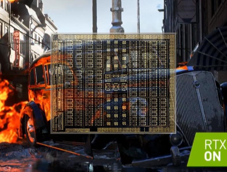
Once again, Nvidia veered in a different direction with its Turing architecture. The addition of dedicated hardware for ray tracing (RTX) and A.I. (Tesnor Cores) brings real-time ray tracing to the gaming world for the first time. It’s a quantum leap in terms of realistic lighting and reflection effects in games, and a rendering technique Nvidia’s CEO Jensen Huang calls the “Holy Grail” of the graphics industry.
Nvidia first announced Turing as the foundation of new professional Quadro cards, but followed that up the next week with a trio of gaming-focused GeForce RTX cards, the 2070, 2080, and 2080 Ti. While the initial focus was all about ray tracing and AI-assisted super-sampling, Nvidia also promised the RTX 2080 would deliver performance improvements of between 35 and 125 percent compared to the previous-generation GTX 1080. But there was also a fair bit of initial backlash over significant generation-over-generation price increases, which pushed the RTX 1080 Ti Founders Edition card to an MSRP of $1,199, compared to the $699 launch price of the GTX 1080 Ti.
Nvidia’s Turing-based RTX cards also introduced a couple other new technologies to the gaming space. The USB-C-based VirtualLink connector is aimed at next-gen VR headsets, while the NVLink connector replaces SLI as an interconnect for multi-card setups that avoids the bottleneck of PCI-E. But there’s also a price increase involved with NVLink. Nvidia says the required bridge connector will cost $79, compared to the $40 price tag of the high-bandwidth SLI bridge designed for 10-series cards.
MORE: Best Graphics Cards
MORE: Desktop GPU Performance Hierarchy Table
-
abryant Archived comments are found here: http://www.tomshardware.com/forum/id-3407581/history-nvidia-gpus.htmlReply -
kinggremlin So, based on the archived comments, this is the THIRD time this article has been posted since the release of Pascal. Why on earth would you keep recycling this article when nothing has been added to the "history?" Turing has not been released yet, we have no benchmarks. Unless this site has no intention of posting reviews of the Turing cards, there is zero reason to re-re-post this just to add an unreleased architecture on the last slide with no useful or new information.Reply -
bit_user Anyone interested in early GPUs (particularly Nvidia's exotic NV1 and its cancelled successor) would probably find this a worthwhile read:Reply
http://vintage3d.org/nv1.php#sthash.AWlq2ihY.dpbs
He thoroughly explores their unique quadric rendering approach, including its down-sides and how they tried to mitigate.
The author of that site has posted on here, in a previous article about vintage 3D cards. Maybe he'll show up, again. -
Blytz I really love to see a graph of the processing power and memory bandwidth of the evolution of these cards (and throw in the ati/radeons as well) to see when we made leaps or increments and how far it's all come.Reply -
bit_user Reply
This isn't exactly relevant to graphics performance, but still worth a look.21265764 said:I really love to see a graph of the processing power and memory bandwidth of the evolution of these cards (and throw in the ati/radeons as well) to see when we made leaps or increments and how far it's all come.
https://www.karlrupp.net/2013/06/cpu-gpu-and-mic-hardware-characteristics-over-time/
Note that the Y-axis of most plots is in log-scale. Also, even though it's from 2013, he updated it for KNL and Pascal. I just wish he'd update it with Volta.
Edit: If you liked that, you might enjoy his 42 Years of Microprocessor Trend Data. -
Unsal Ersoz Wow, I was a very hardcore gamer back then :)Reply
TNT2 and Voodoo3 were competitors until 3DFX released its January 2000 drivers. I can remember it like yesterday. That miniGL port for the opengl games like half-life, quake and others that is long forgotten basically blew tnt2 to the dust (I owned both of the hardware). At 2000, Nvidia was very incompetitive from the software perspective compared to 3dfx with voodoo3. I remember my GLquake renders 10720fps timelapse while tnt2 was stuck with ~60ish :)
Nice memories. -
samopa I am in 3dfx camp until I had forced to switch to nVidia camp. I owned Voodoo1, Banshee, Voodoo2, Voodoo3 3000, Voodoo5 5500 before finally switch to GeForce 6800 Ultra.Reply
Such a fond memories -
AgentLozen I remember posting a comment on this article the last time it came around.Reply
I mentioned last time that I liked the video game screenshots in the background. It helps put the hardware into perspective. For example, the TNT was meant to play games like Half Life. The TNT2 was built to take on Quake 3.
My unique contribution this time is that I would like to see the date of each card's release on each slide. Some entries have this and others don't. I mentioned perspective in my last paragraph and the same applies here. A good analogy for why the date is important would be like taking a history class and hearing "In 1941, America entered World War 2. A short time later, America found itself in Vietnam." So...... was America in Vietnam in that same decade? In the 1950's? The 1960's? It would help my understanding to have a date.
I did enjoy reading this article even if I've looked at it before. -
Stephen_144 The 3dfx was my second gfx card. My second computer, a Pentium 90, had a Diamond Viper Stealth card which I later upgraded to a 3DFX.Reply
I recall loading Windows for Work groups because I could get a 800x600 resolution all the way up to 256 colors. That was up from 640x480 16 colors in the regular windows 3.0. I recall being amazing all the images and spent the entire day downloading (from my dial up Comp-u-Serve 28k modem) color icons and customizing all my windows to use them. Awww simpler times. -
steve.d.moss Is this another biased article like the one telling us to buy RTX cards without even waiting for concrete proof of performance and at inflated prices? I really hope not.Reply
The history of Nvidias rise to power is far more convoluted and full of lies, skullduggery and deceit than people realise.
Check out Adored TV on YouTube. He did a totally unbiased and crystal clear video on this topic a few months back.
Definitely worth a watch, might even open your eye a little.
