GeForce GTX 580 And GF110: The Way Nvidia Meant It To Be Played
After an arguably disappointing GeForce GTX 480 launch back in March, we knew the company had to be working hard on a successor. Meet its flagship GeForce GTX 580, based on the GF110 GPU. This time around, Nvidia proves the idiom "better late than never."
GF110: Nvidia Gives Fermi A Facelift
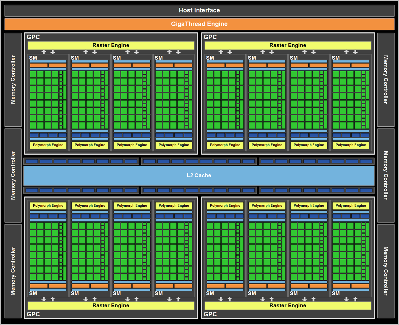
As I’ve mentioned, GF110 is decidedly evolutionary, and Nvidia already had a foundation to build on with GF100, so the number of changes made this time around is actually pretty small. We’re still looking a 40 nm chip consisting of roughly three billion transistors.
First off, the GPU itself is largely the same. This isn’t a GF100 to GF104 sort of change, where Shader Multiprocessors get reoriented to improve performance at mainstream price points (read: more texturing horsepower). The emphasis here remains compute muscle. Really, there are only two feature changes: full-speed FP16 filtering and improved Z-cull efficiency.
GF110 can perform FP16 texture filtering in one clock cycle (similar to GF104), while GF100 required two cycles. In texturing-limited applications, this speed-up may translate into performance gains. The culling improvements give GF110 an advantage in titles that suffer lots of overdraw, helping maximize available memory bandwidth. On a clock-for-clock basis, Nvidia claims these enhancements have up to a 14% impact (or so).
| Header Cell - Column 0 | GeForce GTX 580 | GeForce GTX 480 | GeForce GTX 470 |
|---|---|---|---|
| Graphics Processing Clusters (GPCs) | 4 | 4 | 4 |
| Streaming Multiprocessors (SMs) | 16 | 15 | 14 |
| CUDA Cores | 512 | 480 | 448 |
| Texture Units | 64 | 60 | 56 |
| ROP Units | 48 | 48 | 40 |
| Graphics Clock | 772 MHz | 700 MHz | 607 MHz |
| Shader Clock | 1544 MHz | 1401 MHz | 1215 MHz |
| Memory Clock (Data Rate) | 1002 MHz (4008 MT/s) | 924 MHz (3696 MT/s) | 837 MHz (3348 MT/s) |
| Memory Capacity | 1.5 GB GDDR5 | 1.5 GB GDDR5 | 1.25 GB GDDR5 |
| Memory Interface | 384-bit | 384-bit | 320-bit |
| Memory Bandwidth | 192.4 GB/s | 177.4 GB/s | 133.9 GB/s |
| Fillrate | 49.4 GTexels/s | 42.0 GTexels/s | 34.0 GTexels/s |
| Manufacturing Process | 40 nm TSMC | 40 nm TSMC | 40 nm TSMC |
| Form Factor | Dual-slot | Dual-slot | Dual-slot |
| Display Outputs | 2 x DL-DVI, 1 x mini-HDMI | 2 x DL-DVI, 1 x mini-HDMI | 2 x DL-DVI, 1 x mini-HDMI |
Part of the shift from GF100 to GF110 involves a chip-level re-work. There are different types of transistors an architect can use to build an integrated circuit, depending on the properties he wants to impart. Nvidia’s engineers went back to their GF100 design and purportedly modified much of it, implementing slower, lower-leakage transistors in less timing-sensitive paths and faster, higher-leakage transistors in other areas.
The result was a significant enough power savings to not only allow Nvidia to turn on the 16th Shader Multiprocessor originally disabled in its original design (adding 32 CUDA cores, four texture units, and a single PolyMorph geometry engine), but also ramp up clock rates. Whereas the GeForce GTX 480 sported core/shader/memory frequencies of 700/1401/924 MHz, GeForce GTX 580 employs a 772 MHz core clock, a 1544 MHz shader frequency, and a 1002 MHz memory clock (which translates to a 4008 MT/s data rate). All told, GF110 offers specifications closer to what we were expecting earlier this year. It includes 512 functional CUDA cores, 64 texture units, and 16 PolyMorph engines.
The independent back-end looks the same on a block diagram, the main change being the faster memory clock. It still features six ROP partitions, each associated with a 64-bit memory interface (totaling 384-bit aggregate). Each partition is capable of outputting eight 32-bit integer pixels at a time, totaling 48 pixels per clock.
Telling That Tessellation Tale
Get Tom's Hardware's best news and in-depth reviews, straight to your inbox.
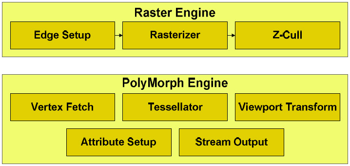
Geometry is suddenly causing quite a stir. When Nvidia briefed us on its Fermi architecture and how it related to gaming, DirectX 11 and tessellation came up over and over. The fact that the company built one of its PolyMorph engines into each of its Shader Multiprocessors (x16 on the GF110 ASIC) would purportedly make a huge difference in titles that extensively utilized tessellation to help increase realism. The problem, of course, was that there weren't any games to show off at the time. Yeah, DiRT 2 and Aliens vs. Predator were out, but both "first-gen" DirectX 11 titles are very choosy in where geometry gets added (neither was able to back Nvidia's claims that more geometry was the future of gaming).
And then there was HAWX 2. The game doesn't actually launch until after the GeForce GTX 580, but a review copy of the game did arrive a couple of days ago. We plan to roll this one into the test suite, just as we used HAWX before it. The controversy, it seems, is that AMD feels HAWX 2 employs an unrealistically high tessellation factor, handicapping the performance of its cards. The company claims to be lobbying for a patch of some sort that'd enable a definable degree of geometry. But once the game starts shipping, with or without the patch, that's the experience available to gamers, and we'll report on it in whichever state it exists.
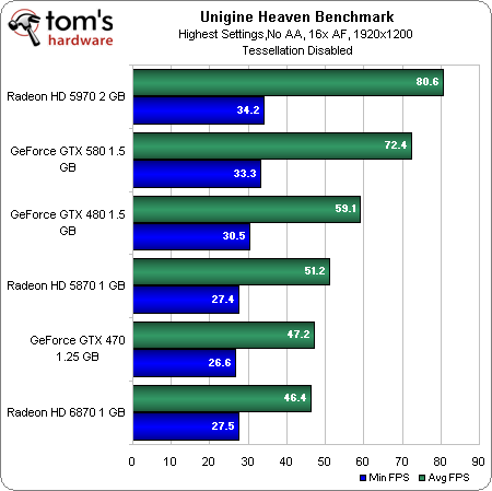
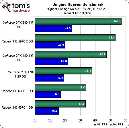
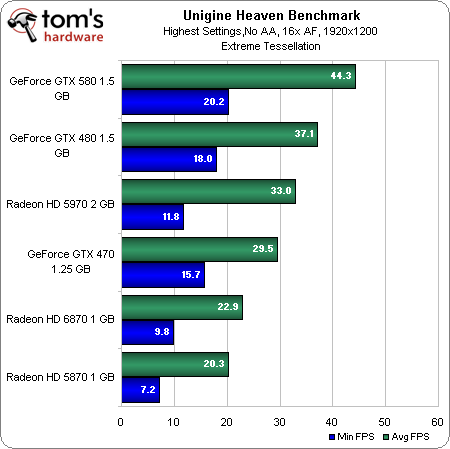
For now, we're using Unigine to measure the scaling performance of each architecture as geometry is ramped up.
Though AMD claims its approach to tessellation is the right one, it's pretty clear that as complexity increases, Nvidia's design maintains more of its performance. The extra SM (and PolyMorph engine) works in concert with higher clocks to give the GeForce GTX 580 a fairly commanding win over the 480 with tessellation set to Extreme in this test. The Radeon HD 5870 can't even keep up with Nvidia's GeForce GTX 470 once complexity is cranked up.
Also interesting is the fact that AMD's Radeon HD 6870 outperforms the technically more capable 5870. AMD claimed that tessellation performance was one of the attributes it worked on with the Barts GPU, and despite its shader deficiency, the newer card finishes ahead (and with a higher minimum frame rate).
Current page: GF110: Nvidia Gives Fermi A Facelift
Prev Page GeForce GTX 580 Goes To Eleven Next Page GeForce GTX 580: Similar Dimensions, Improved Design-
KT_WASP The last bit of the article is the most important I think. Anyone who drops $500 on this card right now, before Cayman releases, should have their head examined. With two companies releasing so close together, it would be in a person's best interest to see what the other is bringing to the table before shelling out such a large chunk of change.Reply
If the 6850 and 6870 have shown one thing.. they are much better then the last gen in many ways (power, noise and scaling) and the cayman is much more robust then the barts. So, before you start calling a winner here, wait and see. That is my advise. -
awood28211 Sound performance but the game here seems to be...double leap-frog. You can just release a product that competes with the competitors current offerings, you gotta compete with what he releases next... If AMD's next offering is significantly faster than it's current, then NVIDIA will still be playing catchup.Reply -
Wheat_Thins Kinda pointless article other then the fact that the 580 offers superb performance but until I see power and noise set in stone I honestly don't care.Reply
A single GPU nearly outperforming a 5970 is quite a statement. Wonder if AMD has what it takes to answer this as the 6850 IMPO is pretty disappointing other then the price. -
nevertell So it's basically what the 480 should have been. Fair enough, I'll wait for the 470 version of the gf110 and buy that.Reply -
TheRockMonsi The price right now for this card is way over $500 on newegg. For that price NVIDIA better be giving me a bj as well.Reply -
It'll certainly be interesting, even if i don't agree with NVIDIA playing catchup. The 480 had its flaws, but it still was the fastest single GPU around.Reply
We'll see what the 69xx have to offer. NVIDIA releasing now puts somewhat of a time constraint on AMD though. If it takes them too long to get something out the door, even some people waiting now may just get the 580 for christmas. -
kevin1212 Nvidia is embarrassed by the power draw of the gtx 580, haha. Improvement in performance but uses the same amt of power... still not a big enough improvement in efficiency, and no big leap in value either. AMD will wipe the floor with this card.Reply
By the way, i know you guys decided to drop crysis, and i can understand that, but given that this is a high end card, maybe you should have considered it, since frankly anyone buying a card like this would probably want it for crysis more than anything else. A 6870 is more than enough for the others. -
iamtheking123 Looks to me that the 580 is somewhere between a 5870 and a 5970. Might have been more impressive if it was Q2 2010 and not Q4 2010.Reply
With ATI's meat-and-gravy bits of the 6000 series on the launchpad, you'd be an idiot to buy one of these at this price.
