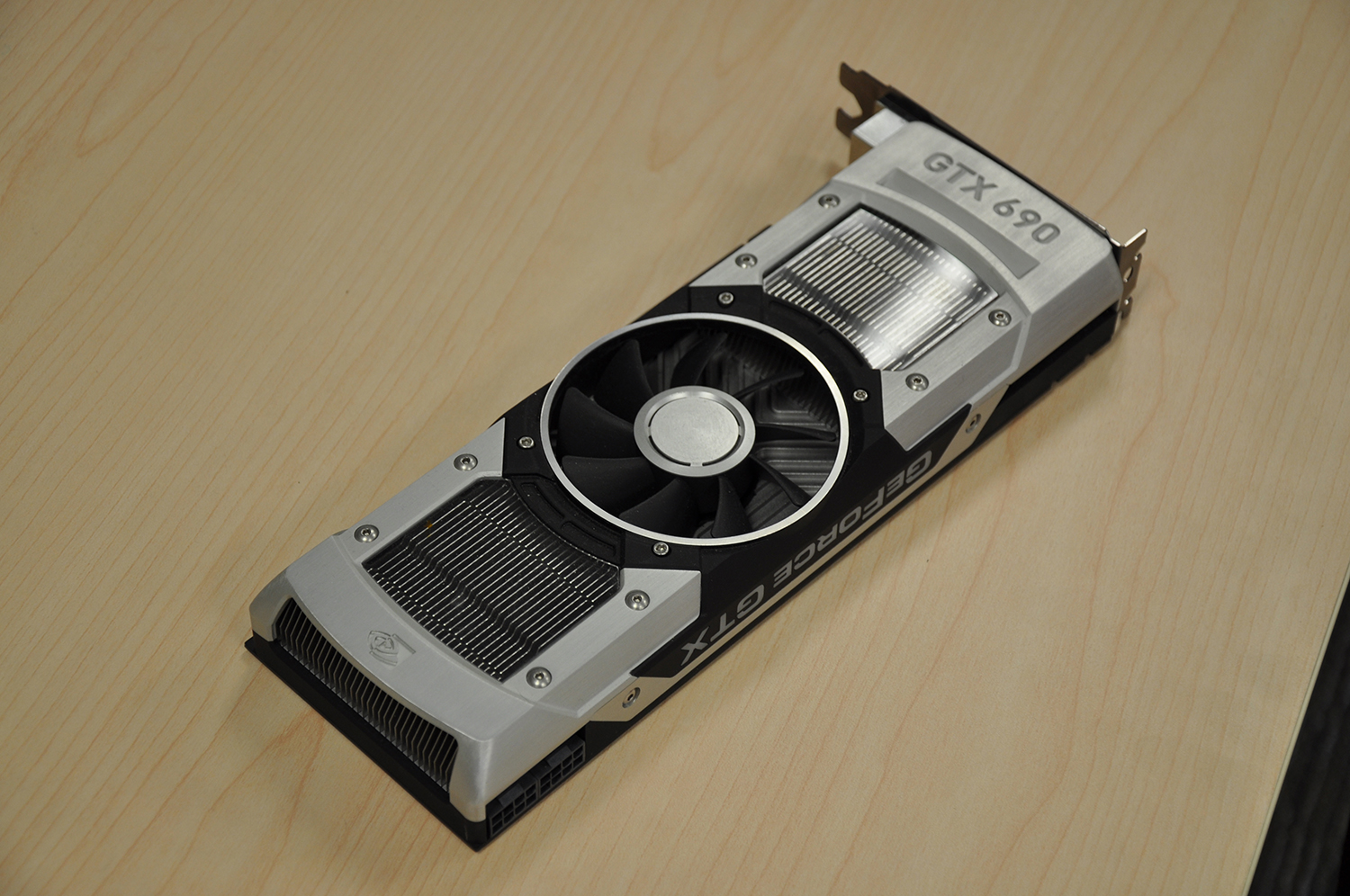
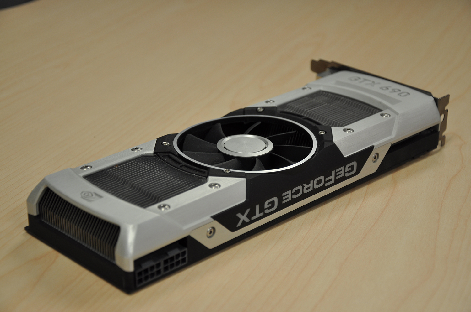
The Story Of How GeForce GTX 690 And Titan Came To Be
When something impresses me, I want to know more, whether it's wine, music, or technology. Months ago, Nvidia dropped off its GeForce GTX 690 and I didn’t know whether to game on it or put it in a frame. This is the story of its conception.
From The Top: Shipping The Hunter Before The Tank
Back in the GeForce GTX 400 and 500 days, Nvidia’s marketing came out with this analogy that resonated with me as a recovered WoW addict. It referred to its highest-end parts leveraging GF110 as “tanks,” meaning they came equipped with all of the compute performance and gaming potential enabled by the Fermi architecture. Later, the GF104-based GeForce GTX 460 surfaced with resources better-suited for playable frame rates, sacrificing most of the bigger chip’s double-precision units in the interest of a leaner GPU. The team used the term “hunter” for that one.
Fast-forward to the Kepler generation. When Nvidia introduced GeForce GTX 680, revealed its GK104 roots, and didn’t discuss compute performance at the launch event, everyone suspected something higher-end was waiting in the wings. As we now know, Nvidia needed around 18,000 GK110s to sell to the government in the form of Tesla cards. So, it made the decision to take GK104 to market first, not necessarily knowing how the card that later became GeForce GTX 680 would fare against AMD’s best effort. In retrospect, its approach paid off. But it could have just as easily gone badly.
Nvidia was working on GK110 all the while, and the processor certainly presented significant technical challenges. The original (65 nm) GT200 GPU at the heart of GeForce GTX 280 measured 576 square millimeters. GK110 covers a still-gargantuan 551 mm², but is also composed of 7.1 billion transistors to GT200’s 1.4. I’ve been told that GK110 is the largest chip that TSMC could fabricate at 28 nm, even. So, looking back, delaying Nvidia’s “tank” in the desktop space allowed the company to do the engineering necessary for a high-performance GPU that behaves well thermally and acoustically.
Article continues belowThat’s not to say Nvidia’s decision makers knew this was going to be the case right away. Having just come from Fermi (which you’ll remember drove the infamously-hot GeForce GTX 480), Andrew’s team saw the size of the chip Jonah’s team was working on and immediately assumed that GK110 would be a 300 W GPU. The GPU engineers were confident that Kepler would be more power-efficient though, and, in the end, GeForce GTX Titan with its one disabled SMX hit the 250 W Nvidia’s board guys were hoping for.
The board team also planned for GeForce GTX 680’s GK104 processor to be a 250 W part, anticipating that it’d replace GeForce GTX 580’s GF110 at 244 W. As we discovered last March, though, the 680 ended up with a 195 W TDP, pushing up to 225 W or so through GPU Boost. But Andrew and Jonah admit to quite a bit of shared stress at the time, as engineers grappled with the previous generation’s power difficulties, what they believed Kepler could do for efficiency, and AMD’s high-profile transition to the powerful GCN architecture, all at the same time.
Get Tom's Hardware's best news and in-depth reviews, straight to your inbox.
Current page: From The Top: Shipping The Hunter Before The Tank
Prev Page Want To Know The Back-Story Of GeForce GTX 690 And Titan? Next Page “The 250 W ID”: Making A Graphics Card Sexy-
CaptainTom You could build cars that go 300 MPH, get 60 MPG, and are as strong as tanks; but if it costs as much as a house... Who cares? Yeah more money buys more. What is so impressive here?Reply
Granted it sure as hell is more impressive than the gains intel makes every year, but then again everything is impressive compared to that... -
jimmysmitty Reply11631932 said:You could build cars that go 300 MPH, get 60 MPG, and are as strong as tanks; but if it costs as much as a house... Who cares? Yeah more money buys more. What is so impressive here?
Granted it sure as hell is more impressive than the gains intel makes every year, but then again everything is impressive compared to that...
If you consider that Intel is working in a much tighter TDP then it makes sense as to why they don't have massive jumps every year. With the ability to throw billions of transistors due to the 2-3x TDP, you can fit more and more every time you do a die shrink in the same area.
As well, it's not like AMD is pushing Intel to do much anyways. FX is not competitive enough to push the high end LGA2011 setup and barley pushes LGA1155 let alone 1150.
As for the design, I will admit it is beautiful. But my one issue is that with said aluminum shroud comes more weight and with more weight means more stress on the PCIe slot. Cards are getting bigger, not smaller. I remember when I had my X850XT PE. It took up one card slot and was a top end card. Even the X1800 took only one sans non reference designs. Now they take up two minimum and are pushing into 3. My 7970 Vapor-X pushes into the 3rd slot and weight a lot too.
Soon we will have 4 slot single GPUs that push into the HDD area. -
bystander @the aboveReply
Realize that GPU's do parallel processing, and a good chunk of the improvements on GPU speed is due to adding more and more processors and not just speeding up the processor itself. Intel works with CPU's, which do linear operations, and they cannot just add more processors and speed things up.
Imagine if CPU's could just add more cores and each core automatically sped things up without having to code for it. That is what GPU's can do and that is why they have been able to advance at a faster rate than CPU's. -
CaptainTom ^ Yes but Intel could get rid of the HD 4600 on the desktop i5's and i7's to add more transistors so the thing is significantly faster. Maybe it would use more power, but its better than Haswell's side-grade over Ivy Bridge.Reply -
emad_ramlawi I am AMDer when it comes to GPU`s, but got handed to Nvidia, the Titan and anything chopped off from GK110 looks impressive, its really great that the stock heat sink design is superior from the get-go, notice how many GK110 cards from different manufacturers that looks the same thing with the same heat sink, and usually same price they just slap there label on it, however in the same time, using top-notch material that costs 600-1000 is not evolutionary, and i don't believe in trick-down economy .Reply -
scrumworks Gotta "love" how Tom's is so loyal nvidia fan. Bias will never stop until couple of those key persons leave and I don't see that happening any time soon.Reply -
kartu What a biased article...Reply
690 is a dual GPU card, Titan is not.
690 is about 20% faster than Titan.
NEWSFLASH:
7990 is 25% faster than Titan.
Source: xbitlabs -
yannigr Titan is an impressive card. 690 is an impressive card. 7990 is an impressive card. The 9800 GX2 that I had in my hands 2 years ago was a monster, truly impressive card. If only it had 2GB of memory (2X1)....Reply
Anyway, all those are old news now. The article is interesting but the fact is that we are waiting to see more news about Hawaii and later about Mantle and in a few months about Maxwell. -
iam2thecrowe Reply11632406 said:What a biased article...
690 is a dual GPU card, Titan is not.
690 is about 20% faster than Titan.
NEWSFLASH:
7990 is 25% faster than Titan.
Source: xbitlabs
newsflash, the 7990 is hotter and noisier and suffers from poor frame latency, particularly when running multiple displays where nearly 50% of frames are dropped completely before they reach the monitor.......
Seriously, Toms are more often AMD biased than Nvidia, so Don't complain about just one article.


