Sponsored by Que Publishing
Upgrading And Repairing PCs 21st Edition: Processor Features
Intel Sockets: LGA 775, LGA 1156, LGA 1366, And LGA 1155
Socket LGA 775
Socket LGA 775 (also called Socket T) is used by the Core 2 Duo/Quad processors, the most recent versions of the Intel Pentium 4 Prescott processor and the Pentium D and Pentium Extreme Edition processors. Some versions of the Celeron and Celeron D also use Socket LGA 775. Socket LGA 775, unlike earlier Intel processor sockets, uses a land grid array format, so the pins are on the socket, rather than the processor.
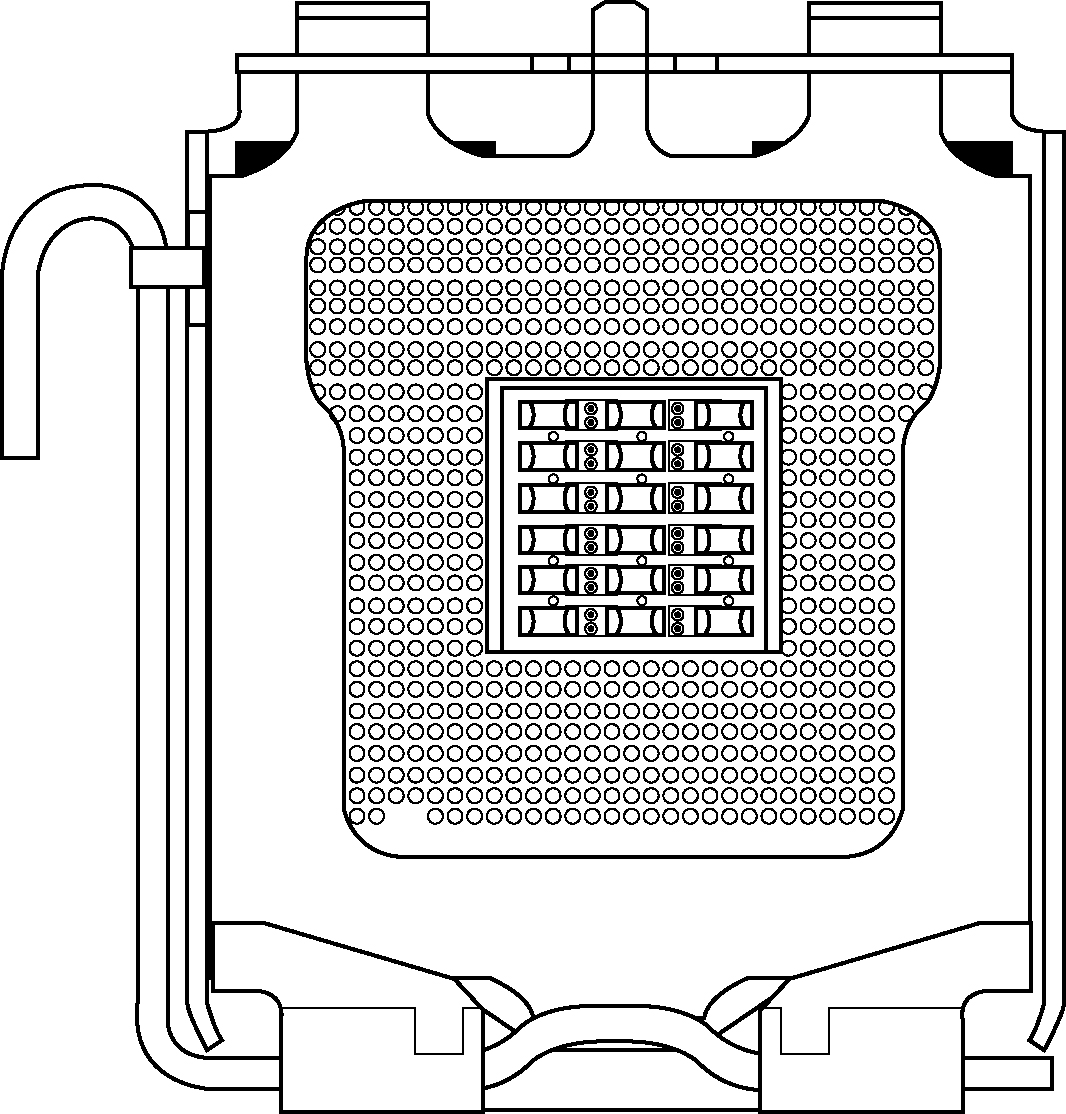
LGA uses gold pads (called lands) on the bottom of the processor to replace the pins used in PGA packages. It allows for much greater clamping forces via a load plate with a locking lever, with greater stability and improved thermal transfer (better cooling). The first LGA processors were the Pentium II and Celeron processors in 1997; in those processors, an LGA chip was soldered on the Slot-1 cartridge. LGA is a recycled version of what was previously called leadless chip carrier (LCC) packaging. This was used way back on the 286 processor in 1984, and it had gold lands around the edge only. (There were far fewer pins back then.) In other ways, LGA is simply a modified version of ball grid array (BGA), with gold lands replacing the solder balls, making it more suitable for socketed (rather than soldered) applications. Socket LGA 775 is shown in the figure below.
The release lever on the left raises the load plate out of the way to permit the processor to be placed over the contacts.
Socket LGA 1156
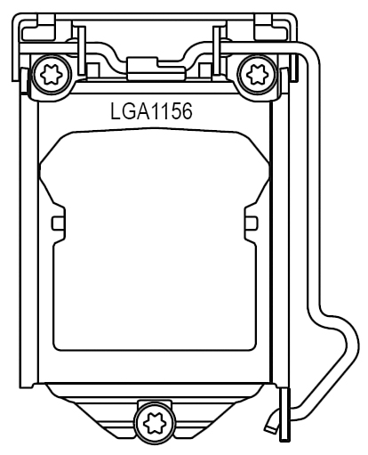
Socket LGA 1156 (also known as Socket H) was introduced in September 2009 and was designed to support Intel Core ix-series processors featuring an integrated chipset northbridge, including a dual-channel DDR3 memory controller and optional integrated graphics. Socket LGA 1156 uses a land grid array format, so the pins are on the socket, rather than the processor. Socket LGA 1156 is shown in the figure below.
Because the processor includes the chipset northbridge, Socket LGA 1156 is designed to interface between a processor and a Platform Controller Hub (PCH), which is the new name used for the southbridge component in supporting 5x series chipsets. The LGA 1156 interface includes the following:
- PCI Express x16 v2.0—For connection to either a single PCIe x16 slot, or two PCIe x8 slots supporting video cards.
- DMI (Direct Media Interface)—For data transfer between the processor and the PCH. DMI in this case is essentially a modified PCI Express x4 v2.0 connection, with a bandwidth of 2 GB/s.
- DDR3 dual-channel—For direct connection between the memory controller integrated into the processor and DDR3 SDRAM modules in a dual-channel configuration.
- FDI (Flexible Display Interface)—For the transfer of digital display data between the (optional) processor integrated graphics and the PCH.
When processors with integrated graphics are used, the Flexible Display Interface carries digital display data from the GPU in the processor to the display interface circuitry in the PCH. Depending on the motherboard, the display interface can support DisplayPort, High Definition Multimedia Interface (HDMI), Digital Visual Interface (DVI), or Video Graphics Array (VGA) connectors.
Socket LGA 1366
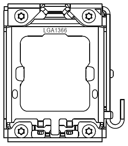
Socket LGA 1366 (also known as Socket B) was introduced in November 2008 to support high-end Intel Core i7-series processors, including an integrated triple-channel DDR3 memory controller, but which also requires an external chipset northbridge, in this case called an I/O Hub (IOH). Socket LGA 1366 uses a land grid array format, so the pins are on the socket, rather than the processor. Socket LGA 1366 is shown in the figure below.
Socket LGA 1366 is designed to interface between a processor and an IOH, which is the new name used for the northbridge component in supporting 5x-series chipsets. The LGA 1366 interface includes the following:
- QPI (Quick Path Interconnect)—For data transfer between the processor and the IOH. QPI transfers two bytes per cycle at either 4.8 or 6.4 GT/s, resulting in a bandwidth of 9.6 or 12.8 GB/s.
- DDR3 triple-channel—For direct connection between the memory controller integrated into the processor and DDR3 SDRAM modules in a triple-channel configuration.
LGA 1366 is designed for high-end PC, workstation, or server use. It supports configurations with multiple processors.
Socket LGA 1155
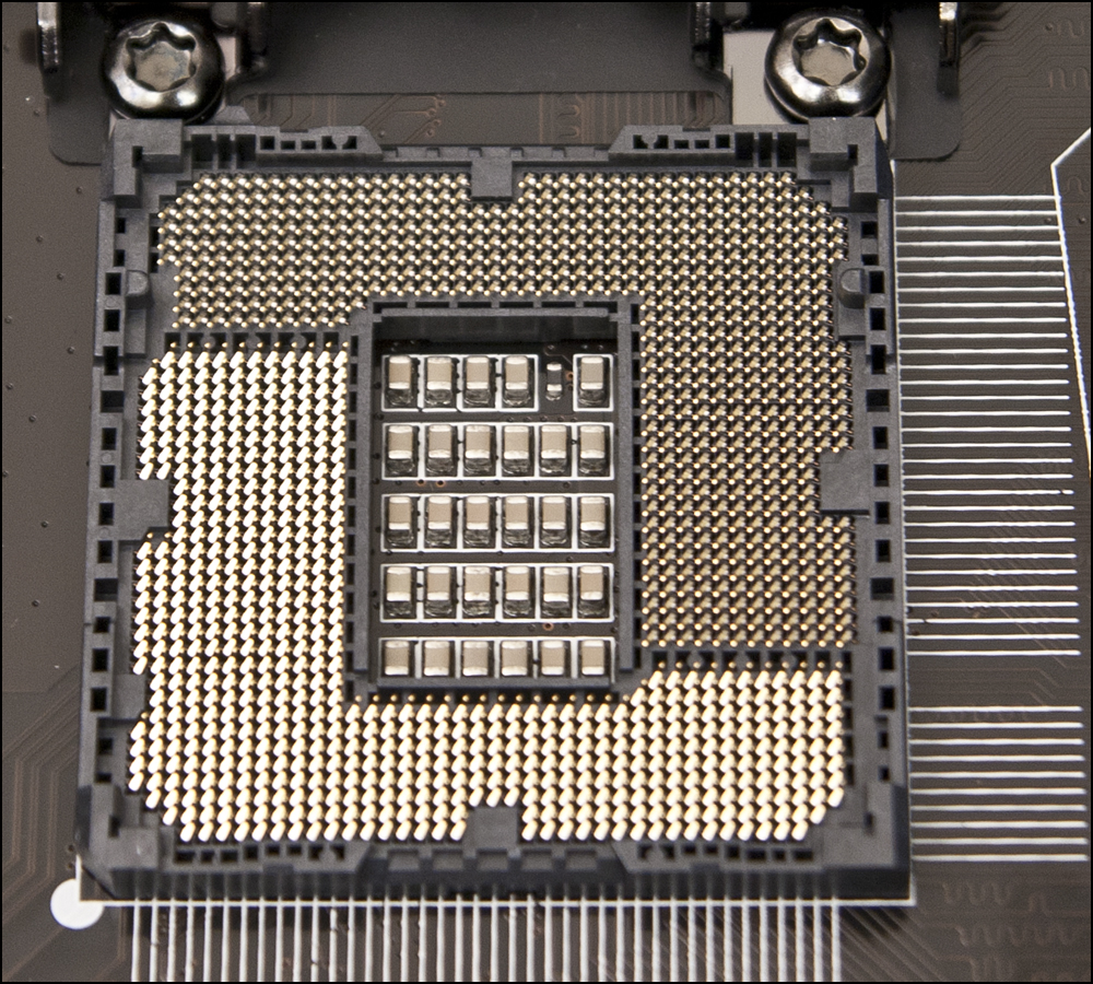
Socket LGA 1155 (also known as Socket H2) was introduced in January 2011 to support Intel’s Sandy Bridge (second-generation) Core ix-series processors, which now include Turbo Boost overclocking. Socket LGA 1155 uses a land grid array format, so the pins are on the socket, rather than the processor. Socket LGA 1155 uses the same cover plate as Socket 1156, but is not interchangeable with it. Socket LGA 1155 is also used by Intel’s Ivy Bridge (third-generation) Core ix-series processors. LGA 1155 supports up to 16 PCIe 3.0 lanes and eight PCIe 2.0 lanes.
Socket LGA 1155 is shown in the figure below.
Socket LGA 2011
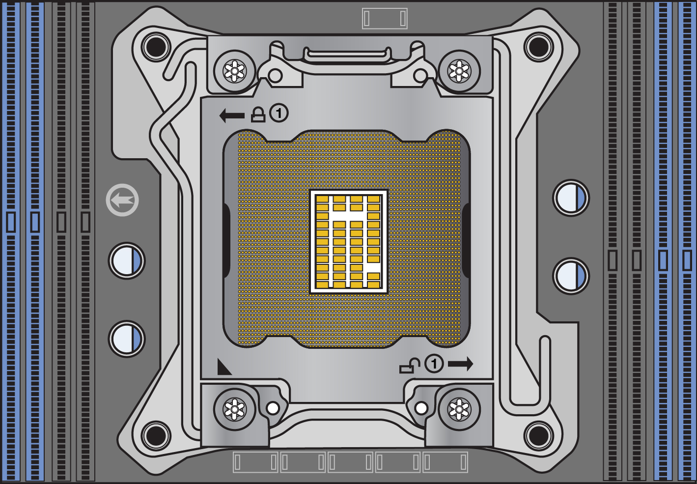
Socket LGA 2011 was introduced in November 2011 to support high-performance versions of Intel’s Sandy Bridge (second-generation) Core ix-series processors (Sandy Bridge-E), which now include Turbo Boost overclocking. LGA 2011 supports 40 PCIe 3.0 lanes, quad-channel memory addressing, and fully-unlocked processor multipliers.
Socket LGA 2011 uses a land grid array format, so the pins are on the socket, rather than the processor. Socket LGA 2011 is shown in the figure below.
Current page: Intel Sockets: LGA 775, LGA 1156, LGA 1366, And LGA 1155
Prev Page Processor Socket And Slot Types Next Page AMD Sockets: AM2/AM2+/AM3/AM3 And F/FM1/FM2Get Tom's Hardware's best news and in-depth reviews, straight to your inbox.
Tom's Hardware is the leading destination for hardcore computer enthusiasts. We cover everything from processors to 3D printers, single-board computers, SSDs and high-end gaming rigs, empowering readers to make the most of the tech they love, keep up on the latest developments and buy the right gear. Our staff has more than 100 years of combined experience covering news, solving tech problems and reviewing components and systems.
-
ta152h Ugggh, got to page two before being disgusted this time. This author is back to writing fiction.Reply
The Pentium (5th generation, in case the author didn't know, thus the "Pent"), DID execute x86 instructions. It was the Pentium Pro that didn't. That was the sixth generation.
CISC and RISC are not arbitary terms, and RISC is better when you have a lot of memory, that's why Intel and AMD use it for x86. They can't execute x86 instructions effectively, so they break it down to RISC type operations, and then execute it. They pay the penalty of adding additional stages in the pipeline which slows down the processor (greater branch mispredict penalty), adds size, and uses power. If they are equal, why would anyone take this penalty?
Being superscalar has nothing to do with being RISC or CISC. Admittedly, the terms aren't carved in stone, and the term can be misleading, as it's not necessarily the number of instructions that defines RISC. Even so, there are clear differences. RISC has fixed length instructions. CISC generally does not. RISC has much simpler memory addressing modes. The main difference is, RISC does not have microcoding to execute instructions - everything is done in hardware. Obviously, this strongly implies much simpler, easier to execute instructions, which make it superior today. However, code density is less for RISC, and that was very important in the 70s and early 80s when memory was not so large. Even now, better density means better performance, since you'll hit the faster caches more often.
This article is also wrong about 3D Now! It was not introduced as an alternative to SSE, SSE was introduced as an alternative to 3D Now!, which predated SSE. In reality, 3D Now! was released because the largest difference between the K6 and Intel processors was floating point. Games, or other software that could use 3D Now!, rather than relying entirely on x87 instructions, could show marked performance improvement for the K6-2. It was relatively small to implement, and in the correct workloads could show dramatic improvements. But, of course, almost no one used it.
The remarks about the dual bus are inaccurate. The reason was that motherboard bus speeds were not able to keep up with microprocessors speeds (starting with the 486DX2). Intel suffered the much slower bus speed to the L2 cache on the Pentium and Pentium MMX, but moved the L2 cache on the same processor package (but not on the same die) with the Pentium Pro. The purpose of having the separate buses was that one could access the L2 cache at a much higher speed; it wasn't limited to the 66 MHz bus speed of the motherboard. The Pentium Pro was never intended to be mainstream, and was too expensive, so Intel moved the L2 cache onto the Slot 1 cartridge, and ran it at half bus speed, which in any case was still much faster than the memory bus.
That was the main reason they went to the two buses.
That was as far as I bothered to read this. It's a pity people can't actually do fact checking when they write books, and make up weird stories that only have a passing resemblance to reality.
And then act like someone winning this misinformation is lucky. Good grief, what a perverse world ...
-
spookyman Yes you are correct on the bus issue. VESA local bus was designed to overcome the limitations of the ISA bus.Reply
As for the reason Intel went with a slot design for the Pentium 2 was to prevent AMD from using it. You can patent and trademark a slot design.
As for the Pentium Pro, it had issues from handling 16bit x86 instruction sets. The solution was to program around it. The was an inherent computational flaw with the Pentium Pro too. -
Kraszmyl I don't think there is a single page that isn't piled with inaccurate or incomplete information.......this is perhaps the worst thing I've ever read on tomshardware and I don't see how you let it get published.Reply -
therogerwilco Kinda nice for generic info, was hoping for more explanation of some of the finer points of cpu architectureReply -
Reynod Perhaps the most important thing to note from this is just how clever some of our users are ... so get into the forums and help out the n00bs with their problems guys !!Reply
:) -
Sprongy Not to be anal but aren't all Core i3 processors, dual cores (2). Some have Hyper-Threading to make it like 4 cores. The last chart above should read Core i3 - 2 cores. Just saying...Reply -
ingtar33 Reply11830610 said:Not to be anal but aren't all Core i3 processors, dual cores (2). Some have Hyper-Threading to make it like 4 cores. The last chart above should read Core i3 - 2 cores. Just saying...
not on mobile. some mobile i3s are single core, same with the mobile i5s... those are all dual core... with hyperthreading.
there are even dual core i5s in haswell on the desktop. (they are the ones with a (t) after the number)
