Sponsored by Que Publishing
Upgrading And Repairing PCs 21st Edition: Processor Features
AMD K10, Bulldozer, Piledriver CPUs, And Fusion/HSA APUs
AMD K10 Processors (Phenom, Phenom II, Athlon II, Athlon X2, Sempron)
The K9 was a stillborn project within AMD, resulting in a skip from the K8 to the K10 architecture. The first K10 processors were the Phenom models released in November 2007.
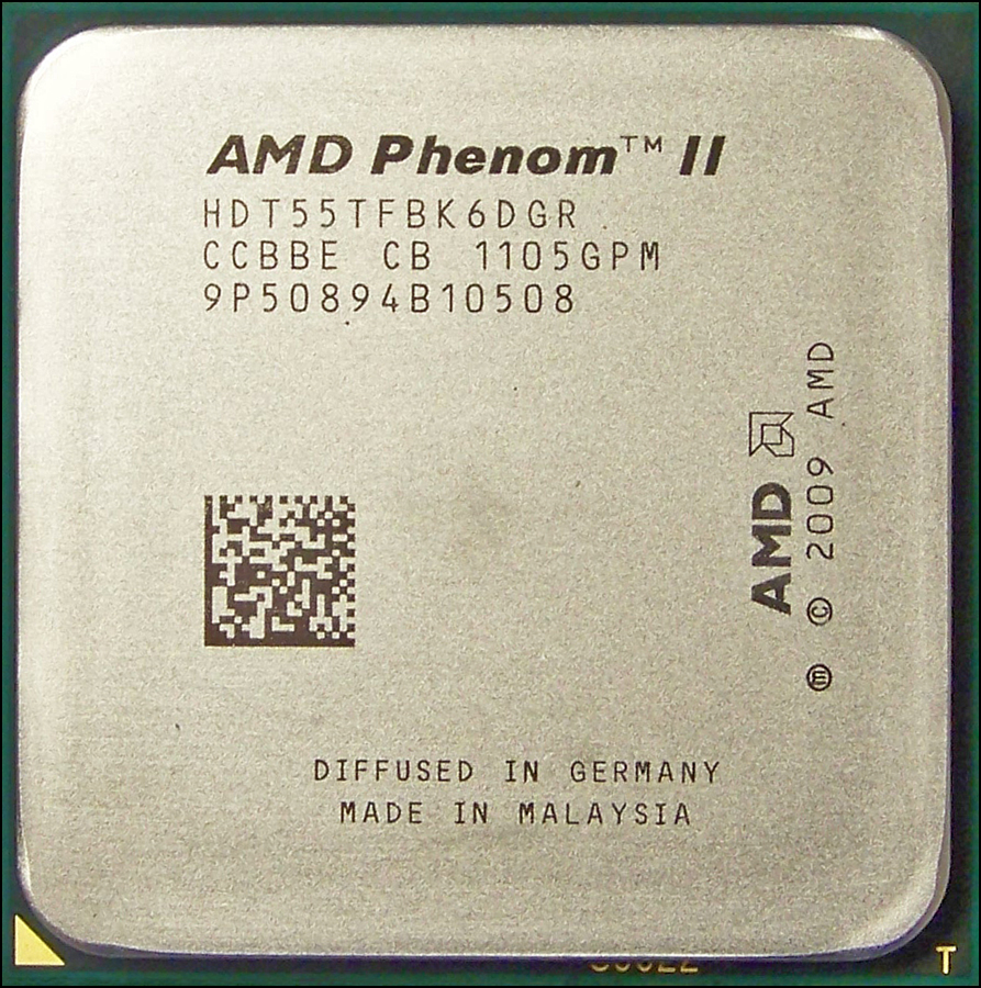
The AMD Phenom family of processors was designed as a flexible family of chips available with 1–6 K10 cores in a single die. These include the Phenom, Phenom II, Athlon II, and some models of the Athlon X2 and Sempron processors. The initial versions used Socket AM2+, which included support for DDR2 memory. Later versions used Sockets AM3 and AM3+, which support DDR3 memory. The image below is of a Phenom II X6 processor for Socket AM3:
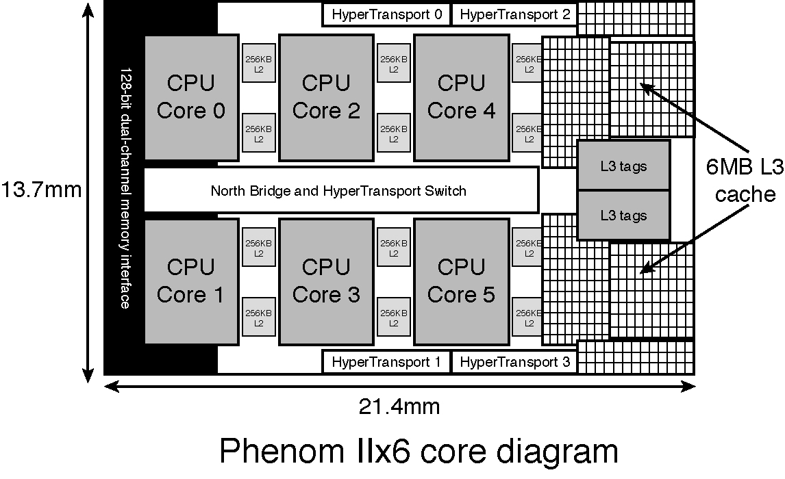
The Phenom X3, X4, and Athlon X2 processors were made on a 65 nm process, whereas the Phenon II, Athlon II, and Sempron 1xx processors use a smaller 45 nm process, resulting in a smaller die with overall lower power consumption and higher performance. The figure below illustrates the interior design of the Phenom II X6 processor:
The higher-end chips in this family include three, four, or six cores, L3 cache, and higher clock rates and HyperTransport bus speeds (2 GT/s).
The table below provides a detailed comparison of the various AMD K10 family processors:
Processor | Cores | CPU Speed | Turbo Core | L2 | L3 | Core | Process | Power | Socket |
|---|---|---|---|---|---|---|---|---|---|
Phenom II X6 | 6 | 2.6-3.3 GHz | Yes | 3 MB | 6 MB | Thuban | 45 nm | 95-125 W | AM3 |
Phenom II X4 | 4 | 2.9-3.5 GHz | Yes | 2 MB | 6 MB | Zosma | 45 nm | 95-125 W | AM3 |
Phenom II X4* | 4 | 2.5-3.7 GHz | No | 2 MB | 4-6 MB | Deneb | 45 nm | 95-140 W | AM3 |
Athlon II X4 | 4 | 2.2-3.8 GHz | No | 2 MB | N/A | Propus | 45 nm | 45-95 W | AM3 |
Phenom II X3 | 3 | 2.4-3.2 Ghz | No | 1.5 MB | 6 MB | Heka | 45 nm | 65-95 W | AM3 |
Athlon II X3 | 3 | 2.2-3.4 GHz | No | 1.5 MB | N/A | Rana | 45 nm | 45-95 W | AM3 |
Phenom II X2 | 2 | 2.8-3.5 GHz | No | 1 MB | 6 MB | Callisto | 45 nm | 80 W | AM3 |
Phenom II X2 | 2 | 3.4 GHz | No | 1 MB | 6 MB | Regor | 45 nm | 80 W | AM3 |
Athlon II X2 | 2 | 1.6-3.3 GHz | No | 1-2 MB | N/A | Regor | 45 nm | 25-65 W | AM3 |
Athlon II 1xxu | 1 | 1.8-2 GHz | No | 1 MB | N/A | Sargas | 45 nm | 20 W | AM3 |
Sempron 1xx | 1 | 2.7-2.9 GHz | No | 1 MB | N/A | Sargas | 45 nm | 45 W | AM3 |
Phenom X4 | 4 | 1.8-2.6 GHz | No | 2 MB | 2 MB | Agena | 65 nm | 65-140 W | AM2+ |
Phenom X3 | 3 | 1.9-2.5 GHz | No | 1.5 MB | 2 MB | Toliman | 65 nm | 65-95 W | AM2+ |
Athlon X2 | 2 | 2.3-2.8 GHz | No | 1 MB | 2 MB | Kuma | 65 nm | 95 W | AM2+ |
*Model 840 has no L3 cache
- Zosma = Thuban with two cores disabled
- Propus = Deneb with no (or disabled) L3 cache
- Heka = Deneb with one core disabled
- Rana = Propus with one core disabled
- Callisto = Deneb with two cores disabled
- Toliman = Agena with one core disabled
- Kuma = Agena with two cores disabled
AM3 processors can also be used in Socket AM2+ motherboards with appropriate BIOS update.
AMD “Bulldozer” and “Piledriver” FX Processors
AMD introduced its follow-up to its K10 architecture, the Bulldozer architecture, in October 2011. Although FX processors in this family use the same Socket AM3+ as late-model K10 processors do, the internal design of Bulldozer processors is very different from its predecessors.
Note: Bulldozer is also known as K11, but Bulldozer is the more common name for this architecture.
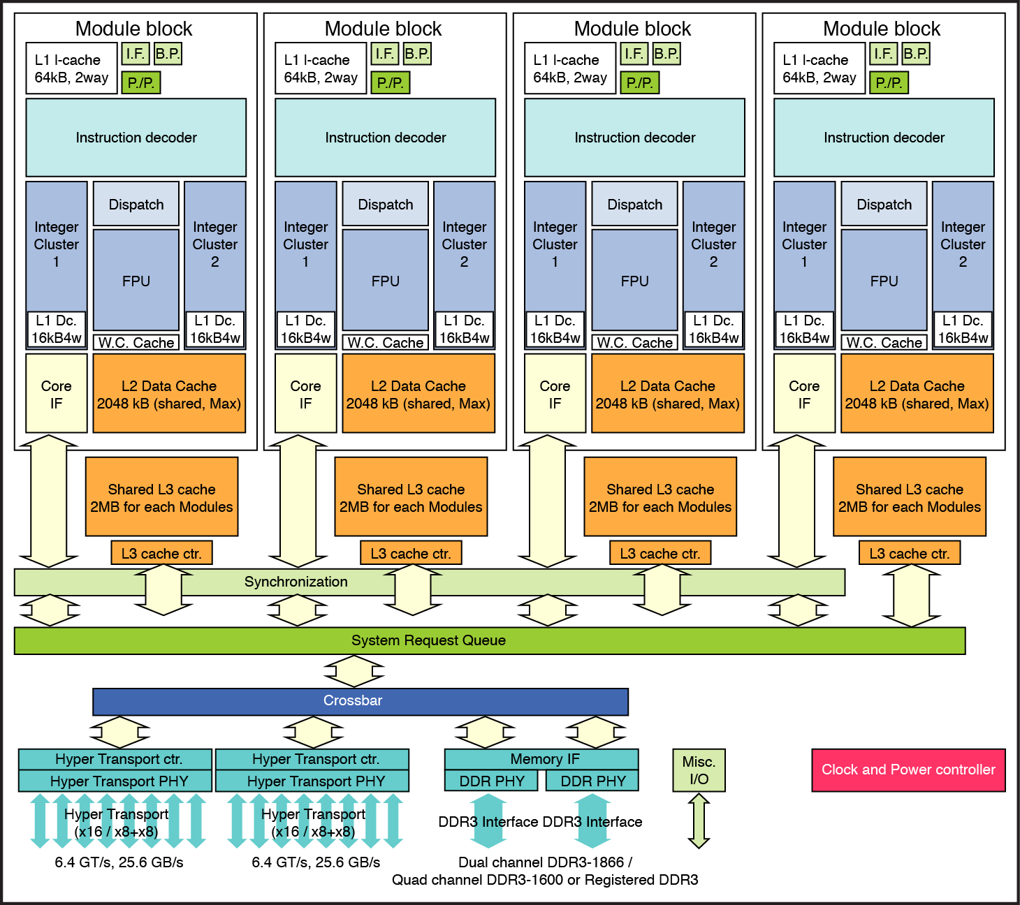
Bulldozer processors are modular. Each module contains a single L1 instruction cache, a multi-branched instruction decoder, and a multilayer dispatch controller. The dispatch controller is connected to two integer processing clusters and a single floating point unit. The results are connected to a write coalescing cache, a core interface unit, and up to 2 MB of L2 cache. A module is commonly referred to as a dual-core processor, although only the integer clusters are dualed. A Bulldozer CPU includes 8 MB of L3 cache memory, and Bulldozer CPUs were manufactured in eight-core, six-core, and four-core versions, known collectively as Zambezi.
Other features in Bulldozer include AMD’s Turbo Core (a built-in overclocking feature) and new CPU instructions (AES, AVX, FMA4, and XOP). These instructions support faster encryption, floating-point math, rendering, and video transcoding on software optimized for them. Bulldozer uses a 32 nm manufacturing process, compared to the 45 nm used by most K10-class parts. FX processors based on Bulldozer are completely unlocked for easier overclocking. AMD sells an optional liquid cooler for FX Bulldozer and Piledriver CPUs.
Bulldozer processors are optimized for multithreaded software, but performance benchmarks were disappointing, as most applications were not optimized for Bulldozer’s new architecture. Further specifications for Bulldozer processers are listed in the table below:
Processor | Cores | CPU Speed | Turbo Core | L2 | Power |
|---|---|---|---|---|---|
FX 81xx | 8 | 3.1-3.6 GHz | Yes | 4 MB | 125 W |
FX 61xx | 6 | 3.3 GHz | Yes | 3 MB | 95 W |
FX 41xx | 4 | 3.8 GHz | No | 2 Mb | 125 W |
AMD introduced an improved version of its Bulldozer architecture, Piledriver, in October 2012. Compared to Bulldozer, Piledriver includes these improvements:
- More accurate branch predictor
- Support for the latest integer instructions FMA4 and F16C
- Improved L1 and L2 cache designs
- Faster clock speeds
The table below lists the FX processors using Piledriver microarchitecture. These processors use the Vishera core.
Processor | Cores | CPU Speed | L2 | Power |
|---|---|---|---|---|
FX 83xx | 8 | 3.5-4 GHz | 4 MB | 125 W |
FX 63xx | 6 | 3.5 GHz | 3 MB | 95 W |
FX 43xx | 4 | 3.8 GHz | 2 MB | 95 W |
AMD Fusion/HSA (Heterogeneous Systems Architecture) APUs
Fusion was the original name for a variety of AMD mobile, desktop, and server processors with in-core graphics, which are now classified under the Heterogeneous Systems Architecture (HSA) designation. AMD refers to these processors as advanced processing units (APUs).
Note: AMD dropped the Fusion name after it was discovered that a Swiss firm, Arctic (originally Arctic Cooling), had been using Fusion for its power supply products since 2006, hence the change to the HSA designation.
AMD has released several lines of APUs, including the C-series (primarily for notebooks) and the E-series (used in notebooks and a few very low-cost desktops). However, the primary product line for desktops is the A-series, which has used two core designs. The initial A-series designs use the Llano core, based on Bulldozer, but with no L3 cache, while the second series uses the Trinity core, based on Piledriver, but again with no L3 cache. The Llano core uses Socket FM1 and includes models with two, three, or four cores and up to 4 MB of L2 cache. The Trinity core uses Socket FM2 and provides faster clock speeds, better GPU performance, and better thermal management. It also features two to four cores with up to 4 MB of L2 cache. The table below compares these processors:
Processor | Cores | CPU Speed | Turbo Core | L2 | GPU | Power | Unlocked | Core |
|---|---|---|---|---|---|---|---|---|
A10-5800K | 4 | 3.8 GHz | Yes | 4 MB | HD 7600D | 100 W | Yes | Trinity |
A10-5700 | 4 | 3.4 GHz | Yes | 4 MB | HD 7600D | 65 W | No | Trinity |
A8-5600K | 4 | 3.6 GHz | Yes | 4 MB | HD 7560D | 100 W | Yes | Trinity |
A8-5500 | 4 | 3.2 GHz | Yes | 4 MB | HD 7560D | 65 W | No | Trinity |
A8-3870K | 4 | 3.0 GHz | No | 4 MB | HD 6550D | 100 W | Yes | Llano |
A8-3850 | 4 | 2.9 GHz | No | 4 MB | HD 6550D | 100 W | No | Llano |
A8-3800 | 4 | 2.4 GHz | Yes | 4 MB | HD 6550D | 65 W | No | Llano |
A6-5400K | 2 | 3.6 GHz | Yes | 1 MB | HD 7540D | 65 W | Yes | Trinity |
A6-3670K | 4 | 2.7 GHz | No | 4 MB | HD 6530D | 100 W | Yes | Llano |
A6-3650 | 4 | 2.6 GHz | No | 4 MB | HD 6530D | 100 W | No | Llano |
A6-3600 | 4 | 2.1 GHz | Yes | 4 MB | HD 6530D | 65 W | No | Llano |
A6-3500 | 4 | 2.1 GHz | Yes | 3 MB | HD 6530D | 65 W | No | Llano |
A4-5300 | 3 | 3.4 GHz | Yes | 1 MB | HD 7480D | 65 W | No | Trinity |
A4-3400 | 2 | 2.7 GHz | No | 1 MB | HD 6410D | 65 W | No | Llano |
A4-3300 | 2 | 2.5 GHz | No | 1 MB | HD 6410D | 65 W | No | Llano |
Current page: AMD K10, Bulldozer, Piledriver CPUs, And Fusion/HSA APUs
Prev Page Intel Core ix-Series And Atom ProcessorsGet Tom's Hardware's best news and in-depth reviews, straight to your inbox.
Tom's Hardware is the leading destination for hardcore computer enthusiasts. We cover everything from processors to 3D printers, single-board computers, SSDs and high-end gaming rigs, empowering readers to make the most of the tech they love, keep up on the latest developments and buy the right gear. Our staff has more than 100 years of combined experience covering news, solving tech problems and reviewing components and systems.
-
ta152h Ugggh, got to page two before being disgusted this time. This author is back to writing fiction.Reply
The Pentium (5th generation, in case the author didn't know, thus the "Pent"), DID execute x86 instructions. It was the Pentium Pro that didn't. That was the sixth generation.
CISC and RISC are not arbitary terms, and RISC is better when you have a lot of memory, that's why Intel and AMD use it for x86. They can't execute x86 instructions effectively, so they break it down to RISC type operations, and then execute it. They pay the penalty of adding additional stages in the pipeline which slows down the processor (greater branch mispredict penalty), adds size, and uses power. If they are equal, why would anyone take this penalty?
Being superscalar has nothing to do with being RISC or CISC. Admittedly, the terms aren't carved in stone, and the term can be misleading, as it's not necessarily the number of instructions that defines RISC. Even so, there are clear differences. RISC has fixed length instructions. CISC generally does not. RISC has much simpler memory addressing modes. The main difference is, RISC does not have microcoding to execute instructions - everything is done in hardware. Obviously, this strongly implies much simpler, easier to execute instructions, which make it superior today. However, code density is less for RISC, and that was very important in the 70s and early 80s when memory was not so large. Even now, better density means better performance, since you'll hit the faster caches more often.
This article is also wrong about 3D Now! It was not introduced as an alternative to SSE, SSE was introduced as an alternative to 3D Now!, which predated SSE. In reality, 3D Now! was released because the largest difference between the K6 and Intel processors was floating point. Games, or other software that could use 3D Now!, rather than relying entirely on x87 instructions, could show marked performance improvement for the K6-2. It was relatively small to implement, and in the correct workloads could show dramatic improvements. But, of course, almost no one used it.
The remarks about the dual bus are inaccurate. The reason was that motherboard bus speeds were not able to keep up with microprocessors speeds (starting with the 486DX2). Intel suffered the much slower bus speed to the L2 cache on the Pentium and Pentium MMX, but moved the L2 cache on the same processor package (but not on the same die) with the Pentium Pro. The purpose of having the separate buses was that one could access the L2 cache at a much higher speed; it wasn't limited to the 66 MHz bus speed of the motherboard. The Pentium Pro was never intended to be mainstream, and was too expensive, so Intel moved the L2 cache onto the Slot 1 cartridge, and ran it at half bus speed, which in any case was still much faster than the memory bus.
That was the main reason they went to the two buses.
That was as far as I bothered to read this. It's a pity people can't actually do fact checking when they write books, and make up weird stories that only have a passing resemblance to reality.
And then act like someone winning this misinformation is lucky. Good grief, what a perverse world ...
-
spookyman Yes you are correct on the bus issue. VESA local bus was designed to overcome the limitations of the ISA bus.Reply
As for the reason Intel went with a slot design for the Pentium 2 was to prevent AMD from using it. You can patent and trademark a slot design.
As for the Pentium Pro, it had issues from handling 16bit x86 instruction sets. The solution was to program around it. The was an inherent computational flaw with the Pentium Pro too. -
Kraszmyl I don't think there is a single page that isn't piled with inaccurate or incomplete information.......this is perhaps the worst thing I've ever read on tomshardware and I don't see how you let it get published.Reply -
therogerwilco Kinda nice for generic info, was hoping for more explanation of some of the finer points of cpu architectureReply -
Reynod Perhaps the most important thing to note from this is just how clever some of our users are ... so get into the forums and help out the n00bs with their problems guys !!Reply
:) -
Sprongy Not to be anal but aren't all Core i3 processors, dual cores (2). Some have Hyper-Threading to make it like 4 cores. The last chart above should read Core i3 - 2 cores. Just saying...Reply -
ingtar33 Reply11830610 said:Not to be anal but aren't all Core i3 processors, dual cores (2). Some have Hyper-Threading to make it like 4 cores. The last chart above should read Core i3 - 2 cores. Just saying...
not on mobile. some mobile i3s are single core, same with the mobile i5s... those are all dual core... with hyperthreading.
there are even dual core i5s in haswell on the desktop. (they are the ones with a (t) after the number)


