Sponsored by Que Publishing
Upgrading And Repairing PCs 21st Edition: Processor Features
AMD Sockets: AM2/AM2+/AM3/AM3 And F/FM1/FM2
Socket AM2/AM2+/AM3/AM3+
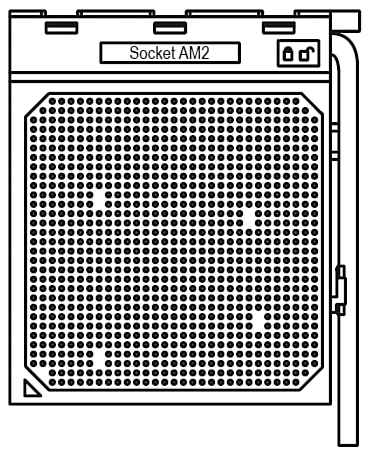
In May 2006, AMD introduced processors that use a new socket, called Socket AM2 (see figure below). AM2 was the first replacement for the confusing array of Socket 754, Socket 939, and Socket 940 form factors for the Athlon 64, Athlon 64 FX, and Athlon 64 X2 processors.
Although Socket AM2 contains 940 pins—the same number that Socket 940 uses—Socket AM2 is designed to support the integrated dual-channel DDR2 memory controllers that were added to the Athlon 64 and Opteron processor families in 2006. Processors designed for Sockets 754, 939, and 940 include DDR memory controllers and are not pin compatible with Socket AM2. Sockets 939, 940, and AM2 support HyperTransport v2.0, which limits most processors to a 1 GHz FSB.
Socket AM2+ is an upgrade to Socket AM2 that was released in November 2007. Although Sockets AM2 and AM2+ are physically the same, Socket AM2+ adds support for split power planes and HyperTransport 3.0, allowing for FSB speeds of up to 2.6 GHz. Socket AM2+ chips are backward compatible with Socket AM2 motherboards, but only at reduced HyperTransport 2.0 FSB speeds. Socket AM2 processors can technically work in Socket AM2+ motherboards; however, this also requires BIOS support, which is not present in all motherboards.
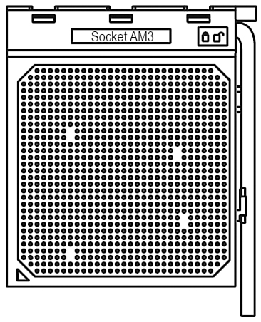
Socket AM3 was introduced in February 2009, primarily to support processors with integrated DDR3 memory controllers such as the Phenom II. Besides adding support for DDR3 memory, Socket AM3 has 941 pins in a modified key pin configuration that physically prevents Socket AM2 or AM2+ processors from being inserted (see figure below).
Socket AM3+ is a modified version of AM3 designed for the new “Bulldozer” processors. It has 938 pins, and also supports processors made for AM3 sockets. The table below shows the essential differences between Socket AM2, AM2+, AM3, and AM3+:
Socket | Pins | Supported Memory |
|---|---|---|
AM2 | 940 | DDR2 (dual-channel) |
AM2+ | 940 | DDR2 (dual-channel) |
AM3 | 938 | DDR3 (dual-channel) |
AM3+ | 938 | DDR3 (dual-cahnnel) |
Here is a summary of the compatibility between AM2, AM2+, AM3, and AM3+ processors and motherboards:
- You cannot install Socket AM2 or AM2+ processors in Socket AM3 motherboards.
- You can install Socket AM2 processors in Socket AM2+ motherboards.
- You can install Socket AM3 or AM2+ processors in Socket AM2 motherboards; however, the BIOS must support the processor, the FSB will run at lower HT 2.0 speeds, and only DDR2 memory is supported.
- You can install Socket AM3 processors in Socket AM2+ motherboards, but the BIOS must support the processor, and only DDR2 memory is supported.
- You can install Socket AM3 processors in Socket AM3+ motherboards, but the BIOS must support the processor.
Although you can physically install newer processors in motherboards with older sockets, and they should theoretically work with reductions in bus speeds and memory support, this also requires BIOS support in the specific motherboard, which may be lacking. In general, you are best off matching the processor to a motherboard with the same type of socket.
Socket F (1207FX)
Socket F (also called 1207FX) was introduced by AMD in August 2006 for its Opteron line of server processors. Socket F is AMD’s first land grid array (LGA) socket, similar to Intel’s Socket LGA 775. It features 1207 pins in a 35-by-35 grid, with the pins in the socket instead of on the processor. Socket F normally appears on motherboards in pairs because it is designed to run dual physical processors on a single motherboard. Socket F was utilized by AMD for its Quad FX processors, which are dual-core processors sold in matched pairs, operating as a dual socket dual-core system. Future versions may support quad-core processors, for a total of eight cores in the system. Due to the high expense of running dual physical processors, only a limited number of nonserver motherboards are available with Socket F.
Socket FM1
Socket FM1 was introduced by AMD in July 2011 for use by accelerated processing units (APUs – CPU plus GPU) and CPUs based on the Llano core. These include the Ax-3xxx series APUs and some Athlon II CPUs, as well as the E2-3200 APU. FM1 has 905 pins in a 31-by-31 grid and uses a PGA socket similar to those used by previous AMD processors. Socket FM1 supports DDR3 memory. It was replaced by Socket FM2.
Socket FM2
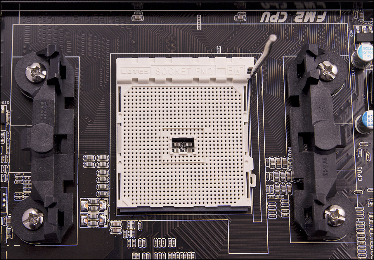
Socket FM1 was introduced by AMD in September 2012 for use by its Trinity series of APUs. These include the Ax-5xxx series APUs. FM2 has 904 pins in a 31×31 grid and uses a PGA socket similar to those used by previous AMD processors. Socket FM2 supports DDR3 memory. The figure below illustrates Socket FM2:
Current page: AMD Sockets: AM2/AM2+/AM3/AM3 And F/FM1/FM2
Prev Page Intel Sockets: LGA 775, LGA 1156, LGA 1366, And LGA 1155 Next Page CPU Operating Voltages And Math Coprocessors (Floating-Point Units)Get Tom's Hardware's best news and in-depth reviews, straight to your inbox.
Tom's Hardware is the leading destination for hardcore computer enthusiasts. We cover everything from processors to 3D printers, single-board computers, SSDs and high-end gaming rigs, empowering readers to make the most of the tech they love, keep up on the latest developments and buy the right gear. Our staff has more than 100 years of combined experience covering news, solving tech problems and reviewing components and systems.
-
ta152h Ugggh, got to page two before being disgusted this time. This author is back to writing fiction.Reply
The Pentium (5th generation, in case the author didn't know, thus the "Pent"), DID execute x86 instructions. It was the Pentium Pro that didn't. That was the sixth generation.
CISC and RISC are not arbitary terms, and RISC is better when you have a lot of memory, that's why Intel and AMD use it for x86. They can't execute x86 instructions effectively, so they break it down to RISC type operations, and then execute it. They pay the penalty of adding additional stages in the pipeline which slows down the processor (greater branch mispredict penalty), adds size, and uses power. If they are equal, why would anyone take this penalty?
Being superscalar has nothing to do with being RISC or CISC. Admittedly, the terms aren't carved in stone, and the term can be misleading, as it's not necessarily the number of instructions that defines RISC. Even so, there are clear differences. RISC has fixed length instructions. CISC generally does not. RISC has much simpler memory addressing modes. The main difference is, RISC does not have microcoding to execute instructions - everything is done in hardware. Obviously, this strongly implies much simpler, easier to execute instructions, which make it superior today. However, code density is less for RISC, and that was very important in the 70s and early 80s when memory was not so large. Even now, better density means better performance, since you'll hit the faster caches more often.
This article is also wrong about 3D Now! It was not introduced as an alternative to SSE, SSE was introduced as an alternative to 3D Now!, which predated SSE. In reality, 3D Now! was released because the largest difference between the K6 and Intel processors was floating point. Games, or other software that could use 3D Now!, rather than relying entirely on x87 instructions, could show marked performance improvement for the K6-2. It was relatively small to implement, and in the correct workloads could show dramatic improvements. But, of course, almost no one used it.
The remarks about the dual bus are inaccurate. The reason was that motherboard bus speeds were not able to keep up with microprocessors speeds (starting with the 486DX2). Intel suffered the much slower bus speed to the L2 cache on the Pentium and Pentium MMX, but moved the L2 cache on the same processor package (but not on the same die) with the Pentium Pro. The purpose of having the separate buses was that one could access the L2 cache at a much higher speed; it wasn't limited to the 66 MHz bus speed of the motherboard. The Pentium Pro was never intended to be mainstream, and was too expensive, so Intel moved the L2 cache onto the Slot 1 cartridge, and ran it at half bus speed, which in any case was still much faster than the memory bus.
That was the main reason they went to the two buses.
That was as far as I bothered to read this. It's a pity people can't actually do fact checking when they write books, and make up weird stories that only have a passing resemblance to reality.
And then act like someone winning this misinformation is lucky. Good grief, what a perverse world ...
-
spookyman Yes you are correct on the bus issue. VESA local bus was designed to overcome the limitations of the ISA bus.Reply
As for the reason Intel went with a slot design for the Pentium 2 was to prevent AMD from using it. You can patent and trademark a slot design.
As for the Pentium Pro, it had issues from handling 16bit x86 instruction sets. The solution was to program around it. The was an inherent computational flaw with the Pentium Pro too. -
Kraszmyl I don't think there is a single page that isn't piled with inaccurate or incomplete information.......this is perhaps the worst thing I've ever read on tomshardware and I don't see how you let it get published.Reply -
therogerwilco Kinda nice for generic info, was hoping for more explanation of some of the finer points of cpu architectureReply -
Reynod Perhaps the most important thing to note from this is just how clever some of our users are ... so get into the forums and help out the n00bs with their problems guys !!Reply
:) -
Sprongy Not to be anal but aren't all Core i3 processors, dual cores (2). Some have Hyper-Threading to make it like 4 cores. The last chart above should read Core i3 - 2 cores. Just saying...Reply -
ingtar33 Reply11830610 said:Not to be anal but aren't all Core i3 processors, dual cores (2). Some have Hyper-Threading to make it like 4 cores. The last chart above should read Core i3 - 2 cores. Just saying...
not on mobile. some mobile i3s are single core, same with the mobile i5s... those are all dual core... with hyperthreading.
there are even dual core i5s in haswell on the desktop. (they are the ones with a (t) after the number)


