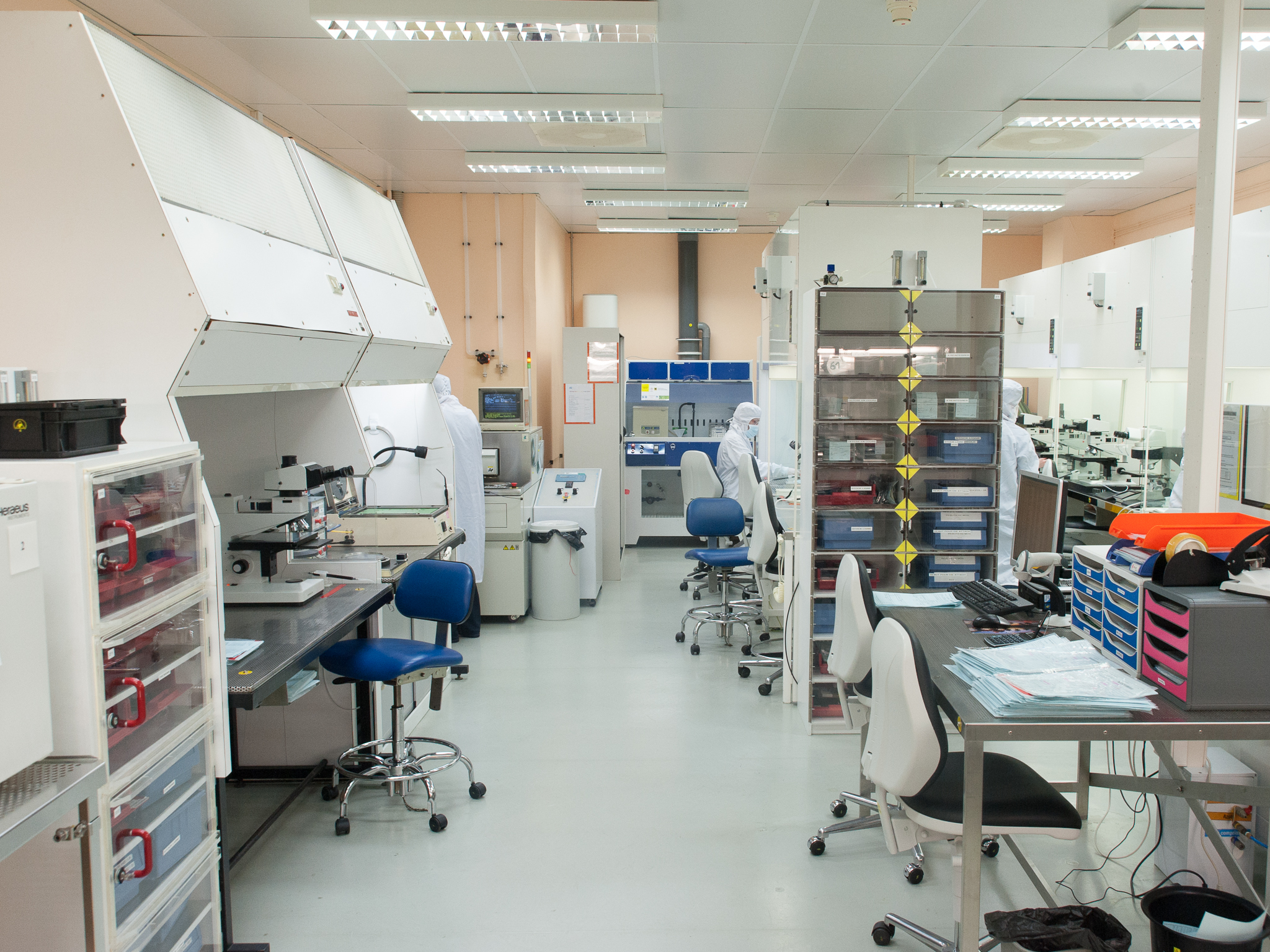
Tom's Hardware Visits STMicroelectronics In Rennes, France
The Beginnings And Development Of The Rennes Back End
The European Space Agency (ESA) was created in 1975 to coordinate the European space programs and certify suppliers authorized to sell their products on that market. Two years later, SGS was the first European supplier to be granted certification. This was first intended for a plant in Italy, but in 1979, that business was moved to Rennes along with the certification.
In 1985, India recognized the European certification, which gave SGS access to the Indian space agency. Japan followed in 1990. So the aerospace activity was already profitable at the time, but growth perspectives were limited by the impossibility of breaking into the American market, which obviously did not recognize the European certification.
STMicro’s El Dorado
So, around 1995, the company decided to work on obtaining American certifications. There are two—one for integrated circuits and the other for dedicated components (diodes, transistors, etc.). STMicroelectronics was granted the former in 2000 after meeting the criteria set by the Defense Logistics Agency of the U.S. Defense Department. Still, it was five or six years before the company was accepted by U.S. manufacturers. The aerospace market is very wary of new arrivals, and certification doesn’t automatically mean you’ll win contracts. You need to build a name and a reputation.
In 2011, STMicroelectronics received the second certification, which entitled the company to sell its entire catalog of products in the U.S. The American market, which then accounted for one to two percent of the aerospace activity’s business volume, now accounts for 25 percent. In short, the development of business at Rennes is the result of greater geographical penetration. And the trend continues. In addition to the U.S., the company is making progress on the Russian and Chinese markets, which have strong growth potential.
Growth Despite Constraints
There are no major differences between American and European certifications, and the components sold in Europe are identical to the ones sold to the U.S. There are slight divergences in the test protocols, but nothing of fundamental importance. Putting up with these bureaucratic disadvantages is the price to pay for being able to sell your products on the world’s markets. And, in fact, it’s one of the strong points of the Rennes site. Few fabs in the world today have all of these certifications.
Get Tom's Hardware's best news and in-depth reviews, straight to your inbox.
During our conversation, we clearly felt that having to manage three quality systems for the same component was a heavy constraint, and Vadrot admitted that if he had a magic wand, his first wish would be to unify the certifications more effectively and make them more consistent. Still, despite these disadvantages, Rennes has not only adapted, but developed itself in order to offer know-how and technologies that make the French plant a leader on the aerospace market. But what, exactly, does the Rennes fab do?
Current page: The Beginnings And Development Of The Rennes Back End
Prev Page History Of The Rennes Site Next Page A Demanding Selection Process-
Scionyde "The poor overall economic picture and pessimistic approach newspapers like to take in speaking of the electronics industry in France would lead you to think that that scenario is utopian at best."Reply
Maybe I'm missing something obvious, but isn't 'utopian' the exact opposite of the word you were intending to use there? -
vancedecker This is really cool. A totally unexpected article in the swamp of cell phone reviews and press releases, on other sites...Reply -
army_ant7 @ScionydeReply
I'm thinking that "utopian" was used in a way to mean something highly unachievable, unlikely, or unfeasible. I'm not sure how that would apply though and I can't speak for the author. I'm not sure if this helps explain that... -
vaughn2k "Once the die is mounted in its case, the wires must be soldered to connect the chip and the pins. This operation can seem archaic compared with the processors used in PCs or smartphones, whose dies are connected via direct contact with bumps on their epoxy carriers." - The wire is not soldered to the pins but welded using an ultrasonic force + power - or Ultrasonic wirebonding. The head of the tool where the wire (either it is an Al or Au wire) comes out, generates this combination of ulrasonic energy to be able to connect the die pad and pins. If an Au wire is used, the process adds a thermal property, which is also called thermosonic bonding. CPU and smart phone chips (and virtually all chips) uses the same process. However, most assembly uses Au wire or Cu wire, instead of Al wire. Another process that is used o intorconnect chips to substrate is called flip-chip bonding, or soldering or ILB (inner lead bonding), and then going into the process of underfilling, to protect these interconnects.Reply -
vaughn2k "The testing also checks for the presence of particles inside the packages" - It is called PIND test (Particle Impact Noise Detection). It is in MIL-STD 883E method 2020.8 -- ;)Reply -
WyomingKnott What double-post? I don't see one.Reply
More practically, you should be able to delete your own post by going to the forum version of the comments. Click on the blue icon with quotation marks, full-edit the duplicate post, and there should be a delete button. -
Hey, and what about Goodram? Isn't it the last european based manufacturer of ram, flash, ssd etc? Can you please make a small trip there as well?Reply
