Tom's Hardware Visits STMicroelectronics In Rennes, France
A Demanding Selection Process
In the jargon of semiconductor manufacturers, the back end is all the stages of fabrication that come after the etching of the transistors onto the wafer of silicon (the front end). A naked die serves no purpose. It has to be protected and connected to the outside world. To do this, the die is soldered into a case or package, and its microscopic interfaces are connected to pins of a size that can be more easily handled.
Rennes receives its wafers from other STMicroelectronics fabs around the world (mainly Singapore, Tours, and Catania). But they’re not ordinary wafers. They’re already suited to aerospace requirements. The Rennes site has no R&D center, but it does have a radiation expert who works with the laboratories at the front-end plants to design chips that are capable of withstanding the ionizing radiation present in space (the same radiation that was responsible for the failure of Curiosity’s memory chip). They’ve been through their own special development and testing track before leaving the front end.
Preliminary Wafer Selection Tests
Once in Rennes, the wafers are cut into individual dies. STMicroelectronics then takes a sampling of chips that will undergo all stages of manufacturing, and then be irradiated by cobalt-60 sources in special laboratories (not on-site, since the use of a radioactive source requires specific expertise). The goal is to verify that the wafer the chip was taken from meets nominal performance standards. Theoretically, there’s no problem, since it was designed and developed to meet those standards. But if the results are not up to standard, the entire wafer has to be rejected.
The chip maker makes a point of adopting highly demanding selection criteria. They can’t afford to run any risk with a component that must be functional for 15 to 20 years (the life expectancy of a satellite in space). So, it's better to junk an entire wafer than risk a malfunction in a satellite in orbit or a robot on Mars.
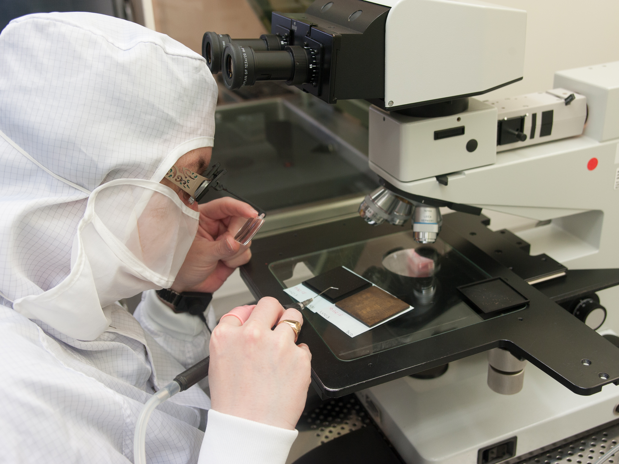
Once the wafer is accepted, it’s cut up (diced) into individual chips. After dicing, each chip is examined under a microscope. The operation requires many different handlings, which limits the production cadence. An operator can sort a maximum of 140 chips per hour, or approximately 1000 chips per day. The selection is rigorous. At this stage, the question is not just whether the chip is functional. A visual defect alone is enough to cause the die to be rejected, even if it’s operational. Here again, the approach is to take zero risk with the final component that will ship.
Rigorous Selection
Get Tom's Hardware's best news and in-depth reviews, straight to your inbox.
If there are any rejects, they mostly occur before packaging of the die. The initial selection criteria are so demanding that the chips that enter the production chain rarely encounter problems. However, the various certifications require that items be taken out of the circuit for testing at each stage of production.
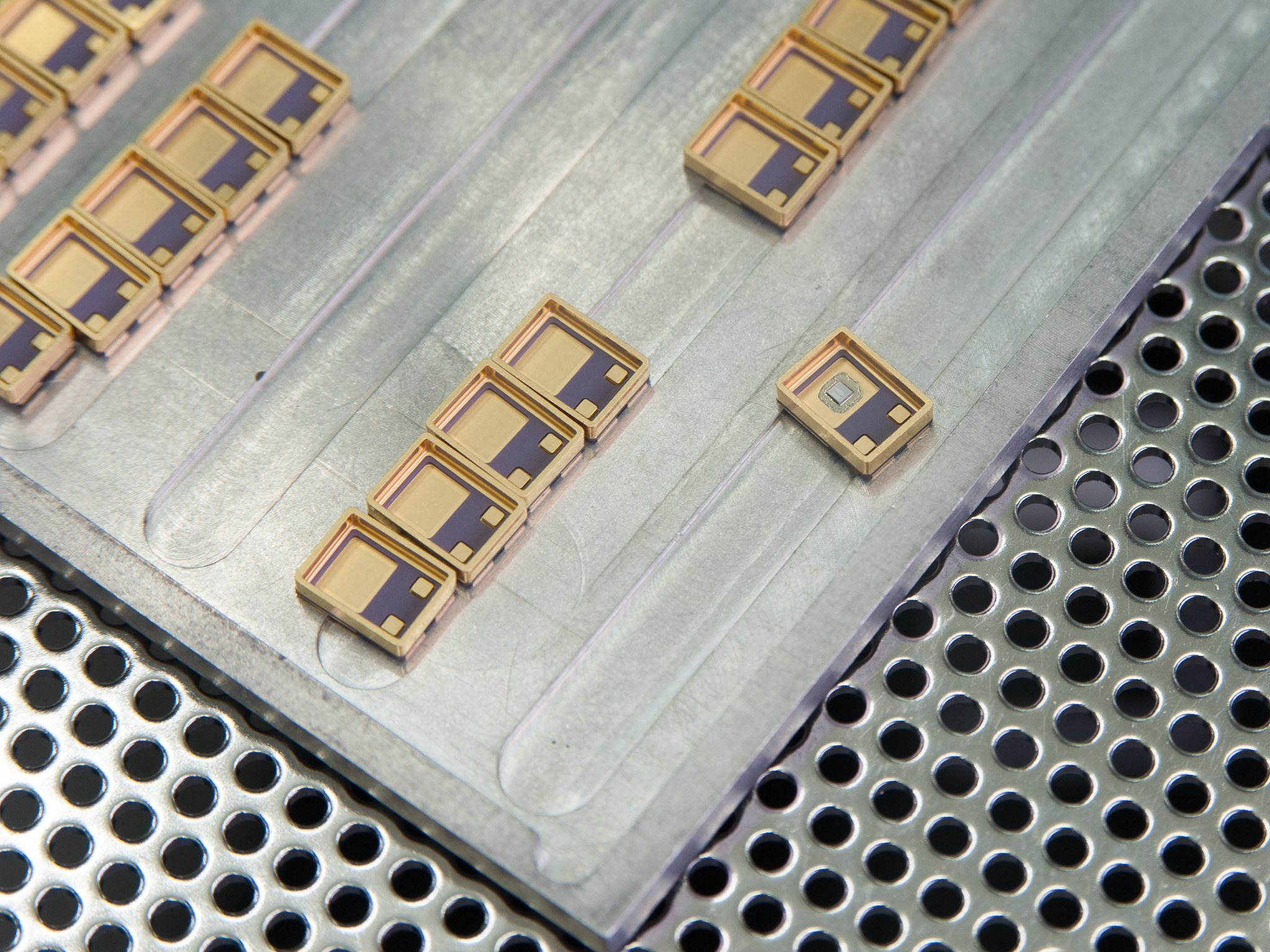
After dicing, the chip is soldered into a case or package. The quality of the assembly is tested—a percentage of the chips are separated out and subjected to a die pull-off test. The packaging used is different from that found in consumer components. Instead of plastic, ceramic is often used—generally alumina (Al2O3) or aluminum nitride (AlN)—or else metal (steel or kovar, which is an alloy of iron, nickel, and cobalt). The choice of the case depends mainly on the type of chip it will house. Chips that need no power will use a ceramic case. Signal processing components, for example, use ceramic. Dies with a Thermal Design Power (TDP) of a few watts, such as power components that require a current of 3 to 5 A and a tension of a few volts, use metal packaging.
Contrary to popular belief, the choice of packaging doesn’t depend on the environment in which the chip will operate. Whether it is used in space or in a drill head 20 km underground, the component will be identical. The high-reliability standards these chips must meet are intended to satisfy operation under any conditions. So the choice of the case depends only on the characteristics of the circuit it houses.
Current page: A Demanding Selection Process
Prev Page The Beginnings And Development Of The Rennes Back End Next Page Highly Rigorous Tests-
Scionyde "The poor overall economic picture and pessimistic approach newspapers like to take in speaking of the electronics industry in France would lead you to think that that scenario is utopian at best."Reply
Maybe I'm missing something obvious, but isn't 'utopian' the exact opposite of the word you were intending to use there? -
vancedecker This is really cool. A totally unexpected article in the swamp of cell phone reviews and press releases, on other sites...Reply -
army_ant7 @ScionydeReply
I'm thinking that "utopian" was used in a way to mean something highly unachievable, unlikely, or unfeasible. I'm not sure how that would apply though and I can't speak for the author. I'm not sure if this helps explain that... -
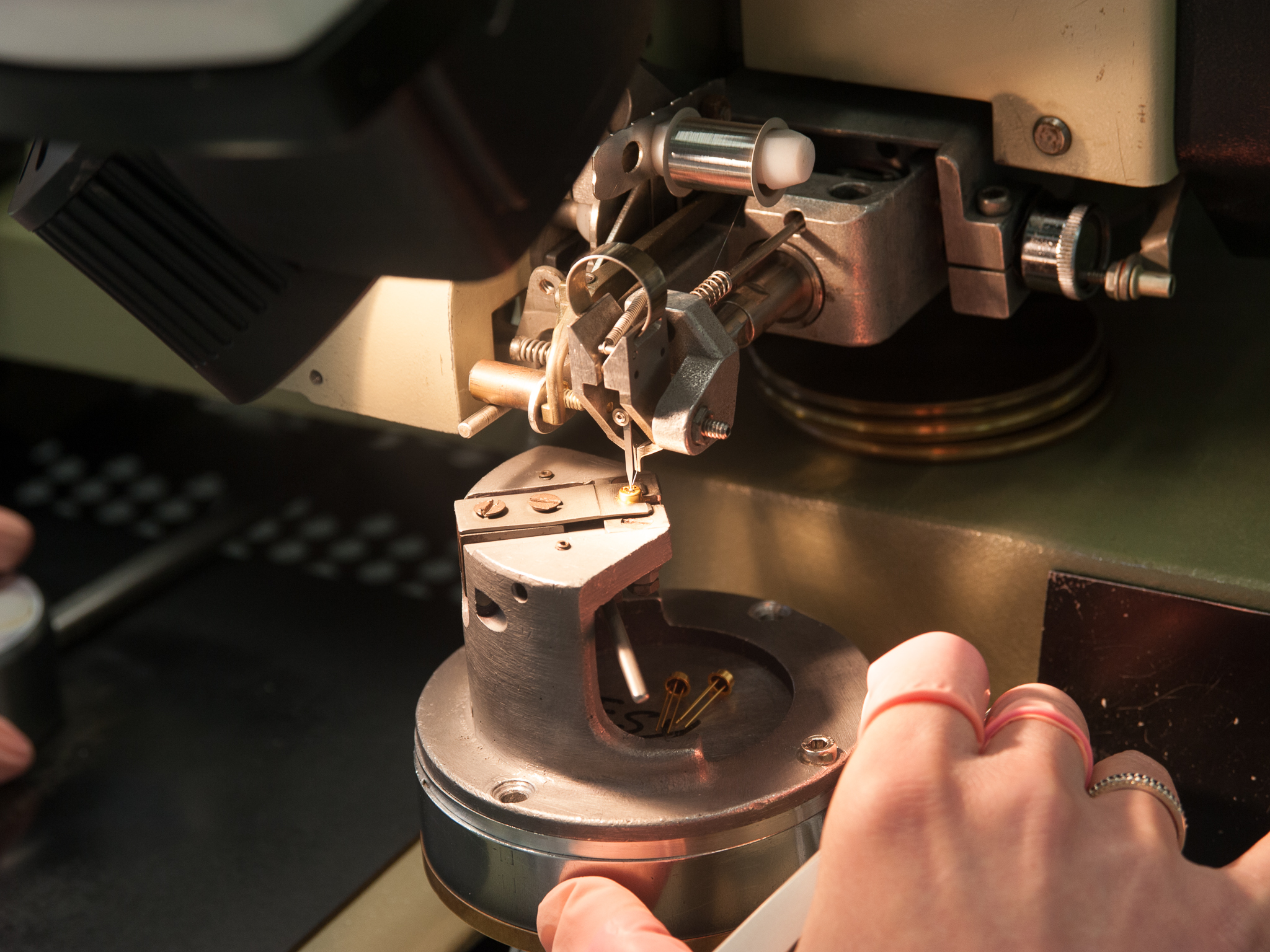
vaughn2k "Once the die is mounted in its case, the wires must be soldered to connect the chip and the pins. This operation can seem archaic compared with the processors used in PCs or smartphones, whose dies are connected via direct contact with bumps on their epoxy carriers." - The wire is not soldered to the pins but welded using an ultrasonic force + power - or Ultrasonic wirebonding. The head of the tool where the wire (either it is an Al or Au wire) comes out, generates this combination of ulrasonic energy to be able to connect the die pad and pins. If an Au wire is used, the process adds a thermal property, which is also called thermosonic bonding. CPU and smart phone chips (and virtually all chips) uses the same process. However, most assembly uses Au wire or Cu wire, instead of Al wire. Another process that is used o intorconnect chips to substrate is called flip-chip bonding, or soldering or ILB (inner lead bonding), and then going into the process of underfilling, to protect these interconnects.Reply -
vaughn2k "The testing also checks for the presence of particles inside the packages" - It is called PIND test (Particle Impact Noise Detection). It is in MIL-STD 883E method 2020.8 -- ;)Reply -
WyomingKnott What double-post? I don't see one.Reply
More practically, you should be able to delete your own post by going to the forum version of the comments. Click on the blue icon with quotation marks, full-edit the duplicate post, and there should be a delete button. -
Hey, and what about Goodram? Isn't it the last european based manufacturer of ram, flash, ssd etc? Can you please make a small trip there as well?Reply


