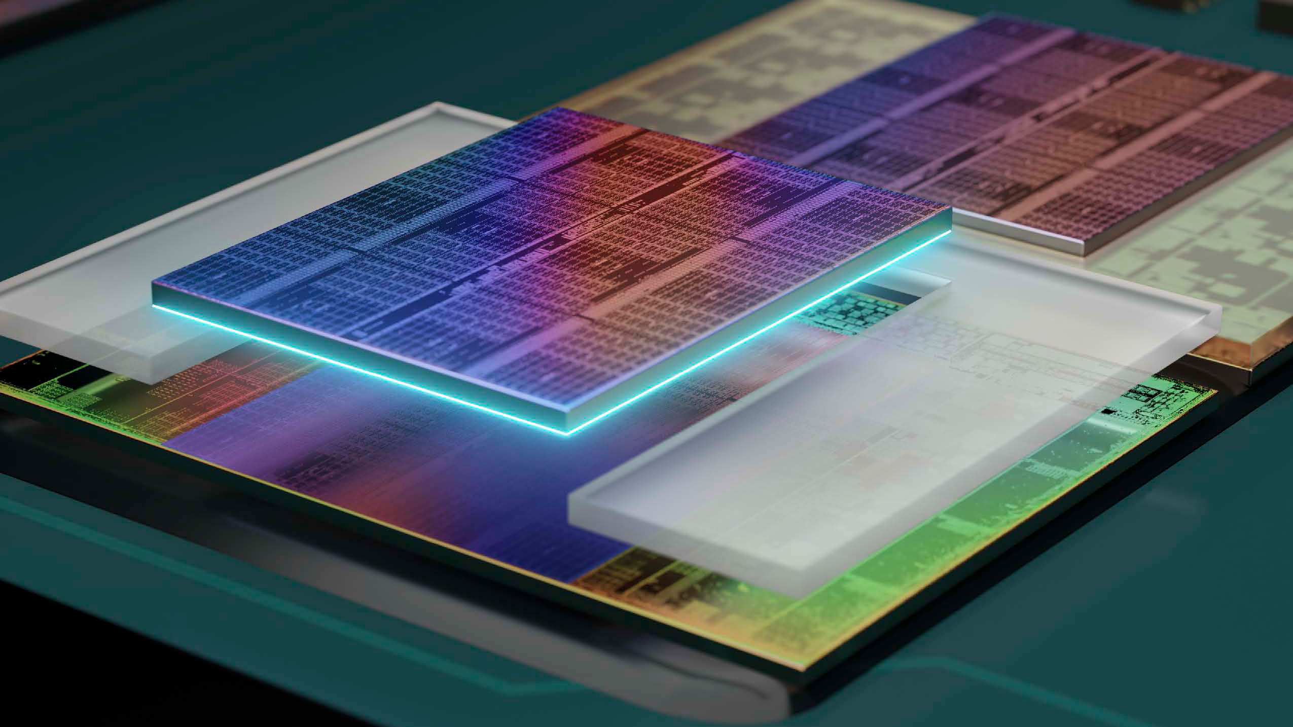
Nvidia Omniverse used by researchers to analyze and improve stacked chip designs in 3D
As chips adopt 3D stacking technologies, designers will need to see these chips in 3D.

Semiconductor chip building is becoming more complex, and a big trend in that direction is the adoption of new 3D-stacking technologies that improve chip density at a level that would be impossible with traditional shipbuilding methods. A blog post by Nvidia's Baskar Rajagopalan reports that engineering simulation and 3D design software company Ansys is using Nvidia's Omniverse platform to analyze 3D-based semiconductor designs in 3D. The company utilizes Nvidia's modulus Fourier neural operator architecture to predict power profiles when developing chip designs.
This technology is very advantageous for chip designers. Viewing a 3D-based chip design in a 3-dimensional space can give engineers a better perspective of how the chip will behave under various conditions. Nvidia provides an example of finding hot spots and rectifying electromagnetic issues faster and more easily in a 3D-stacked chip design when viewed from a 3-dimensional perspective.
A great example of why it is advantageous to see a chip design in 3D is to detect hot spots (as Nvidia suggested) that will inevitably occur between two pieces of silicon 3D stacked on top of one another. Viewing the 3D stacked design from a 3-dimensional view will allow an engineer to detect the exact depth where the hot spot is occurring. In contrast, in a 2D environment (viewing the chip from the top), an engineer would find it more difficult to detect the hot spot since it could occur at the top, middle, or bottom of the chip from a two-dimensional viewpoint.
Ansys also utilizes Omniverse to simulate temperatures across the entire chip to assist with hot spot detection based on various power profiles and floor plans. This can help rectify any thermal issues that might occur with a new 3D chip design before the first prototype is even built.
Ansys will demonstrate its 3D design software in person at the Design Automation Conference this week. On top of this, the company is also working with Nvidia's Modulus Fourier neural operator architecture to create AI-generated tools that assist in testing 3D-stacked chip designs. With Modulus, Ansys researchers created an AI surrogate model that predicts temperature profiles for any given power profile defined by system parameters like heat transfer coefficient, thickness, and material properties.
Chip design is yet another area where businesses are taking advantage of Nvidia's Omniverse platform. The app is already growing in popularity with some of the world's largest manufacturers due to its capabilities to mimic real life in a virtualized 3D environment. Viewing chip designs in 3D is a great idea and will undoubtedly be the way forward for future chip development, particularly 3D stacked chips.
Get Tom's Hardware's best news and in-depth reviews, straight to your inbox.

Aaron Klotz is a contributing writer for Tom’s Hardware, covering news related to computer hardware such as CPUs, and graphics cards.
-
nichrome Indeed, traditional shipbuilding methods just won't cut it . Pretty good imagery, though.Reply -
edzieba Reply
Yeah, when I ran my rough-hewn oak keel spar through the Twinscan EXE:5000, it made a right mess!nichrome said:Indeed, traditional shipbuilding methods just won't cut it . Pretty good imagery, though.