Rambus Outs HBM3 Details: 1.075 TBps of Bandwidth, 16 Channels, 16-Hi Stacks
Moar throughput!
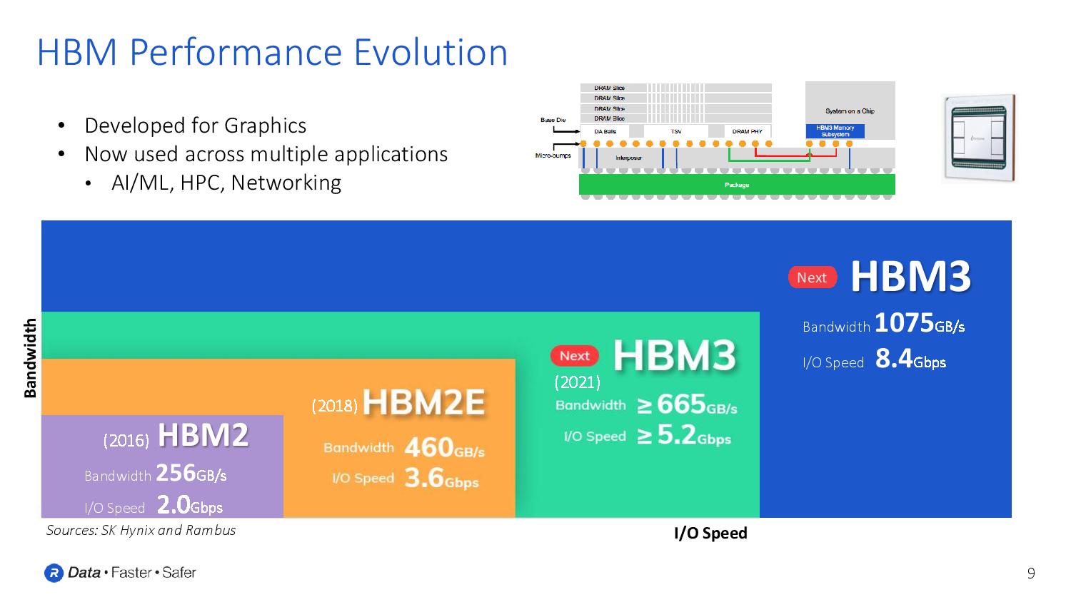
Future GPUs are about to get a whole lot faster. Details of HBM3 have trickled out slowly, with the first vague specs coming from SK hynix. But Rambus' announcement that the company has developed a new HBM3-ready combined PHY and memory controller brings much more information to light. That includes a potential for HBM3 to reach up to 8.4 Gbps-per-pin, 1.075 TB/s of throughput, and support for up to 16 channels of memory and 16-Hi memory stacks. That's more than twice the capacity and bandwidth offered with HBM2E, portending potential radical speedups for tomorrow's GPUs and SoCs.
Like HBM2E, the new HBM3 standard utilizes a 1024-bit wide interface with 64 bits per channel. However, HBM3 supports 16 channels. That's twice the number of channels with HBM2, resulting in the lion's share of the performance improvements, including the more than doubled throughput. Additionally, the architecture also supports a pseudo channel for each channel (up to 32 pseudo channels), allowing for fine-tuning traffic based on the size of memory accesses, which is particularly helpful for AI workloads.
| HBM3 based on Rambus Peak Performance | HBM3 | HBM2 / HBM2E | HBM |
| Max Pin Transfer Rate (I/O Speed) | 8.4 | 3.2 Gbps / 3.65 Gbps | 1 Gbps |
| Maximum Die Per Stack | 4 (4-Hi) | 8 (8-Hi) / 12 (12-Hi) | 16 (16-Hi) |
| Max Package Capacity | 64 GB | 24 GB | 4 GB |
| Max Bandwith | 1075 GBps | 410 / 460 GBps | 128 GBps |
The increased number of memory channels supports more memory die, thus supporting up to 16-Hi stacks (supports up to 32 Gb per channel) that deliver up to 32GB of total capacity, with 64GB of capacity possible in the future.
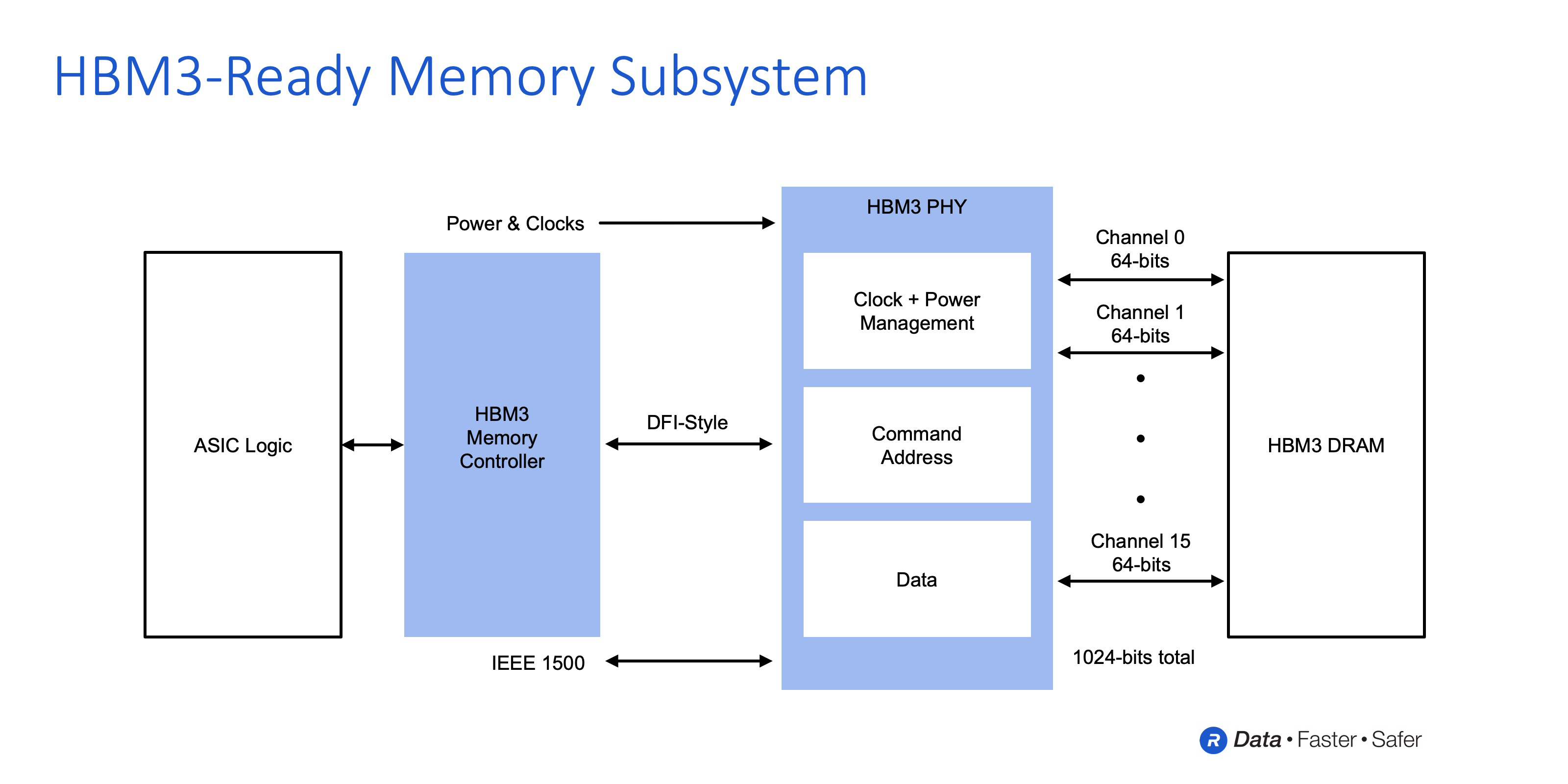
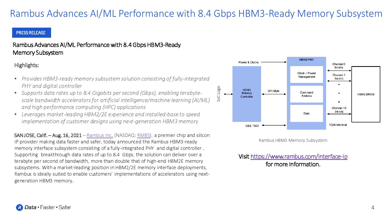
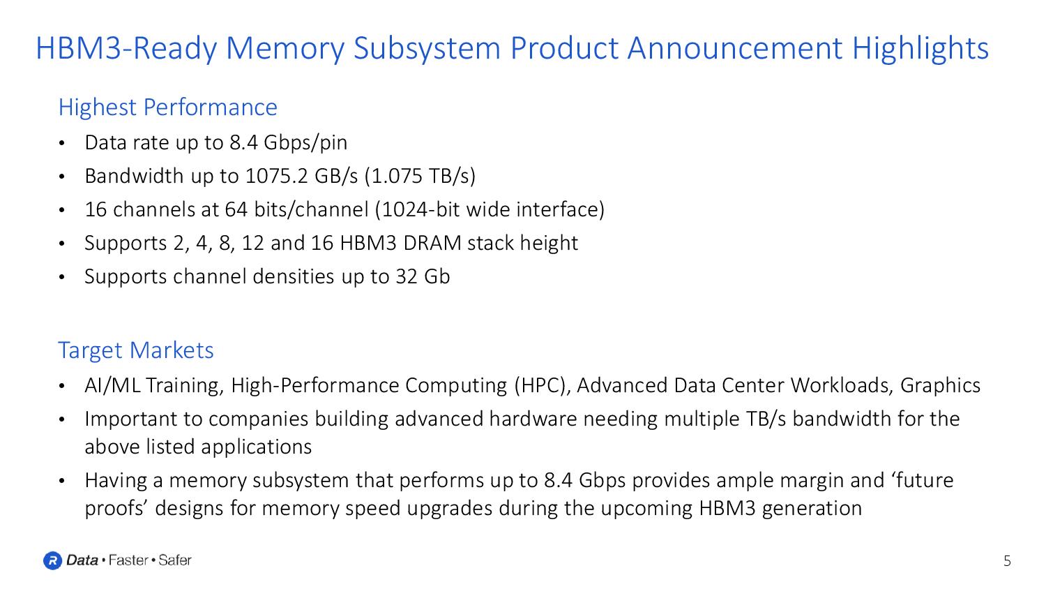
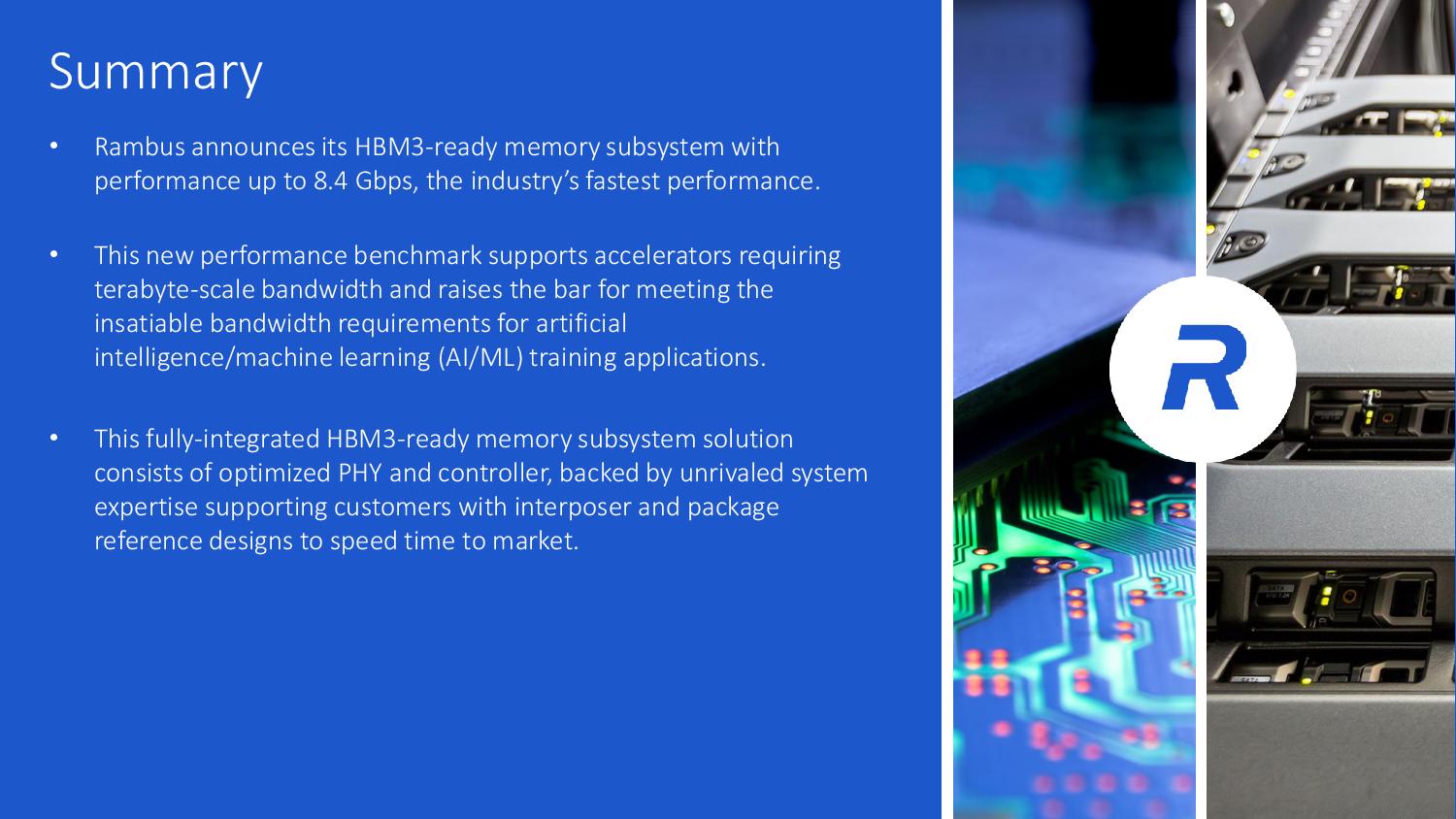

Paired with SK hynix's PHY and memory controller, the company says it plans to hit 1.075 TB/s of throughput and 8.4 Gbps/pin with HBM3. That's more than a doubling of HBM2E's metrics, which weigh in at 460 GB/s and 3.2 Gbps/pin. Notably, these specifications match the heights of the PHY and memory controller's capabilities, but it will take some time for memory vendors to evolve their products to support such speeds. As a result, we should expect somewhat lower performance from the leading-edge products.
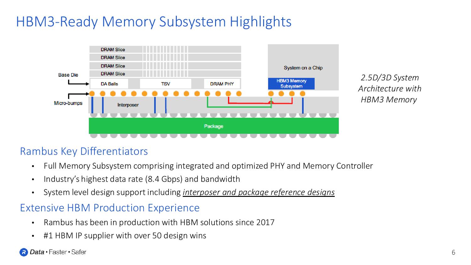
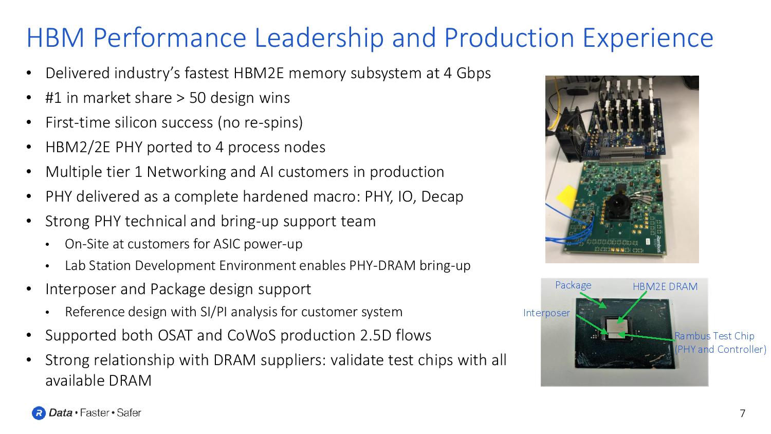
Rambus also provides its customers with reference 2.5D packaging designs (including both interposers and packages) to speed the integration of its PHY and memory controllers into an SoC. These feature what we should consider rather standard interposer designs connected to the memory package via microbumps.
The Rambus offering fully supports the JEDEC spec, so it doesn't support the (for now) exotic HBM-PIM (Processing in Memory) tech that has embedded in-die processing power. Those memories are still in the early stages of industry adoption from several memory manufacturers but are largely thought to be a shoo-in for JEDEC support in the future.
Many details of the actual JEDEC HBM3 spec are still fuzzy, as the standards body hasn't officially made the details public yet. However, the picture is becoming a bit clearer as the ecosystem continues to evolve and players like Rambus and SK hynix begin sharing the preliminary details.
Get Tom's Hardware's best news and in-depth reviews, straight to your inbox.
Rambus tells us that the first SoCs that leverage its design will land either late next year or early 2023, so we expect the formal spec reveal in the coming months.

Paul Alcorn is the Editor-in-Chief for Tom's Hardware US. He also writes news and reviews on CPUs, storage, and enterprise hardware.
-
Soul_keeper The royalties/costs from implementing HBM in products must be off the charts compared to gddr.Reply
We havn't seen many products use it since vega VII and the frontier edition.
It seems like most of this goes into multi-thousand dollar datacenter/compute products anymore. -
Xajel I wish they come with a low-cost HBM implementation.Reply
Samsung once announced an HBM-LC once, but it seems it didn't get much attention and forgot about it.
The main idea is to use a narrower bus, narrower than 1024bit, with lower density to the point it can be used on regular organic packaging rather than requiring an expensive silicon interposer. But it seems that the total cost will be questionable compared to GDDR6 which can use even cheaper implementation (just in PCB), so the space-saving that HBM brings isn't worth it after all.