Researchers Can Now Reverse Engineer Entire Chips With X-Ray Technology
Get Tom's Hardware's best news and in-depth reviews, straight to your inbox.
You are now subscribed
Your newsletter sign-up was successful
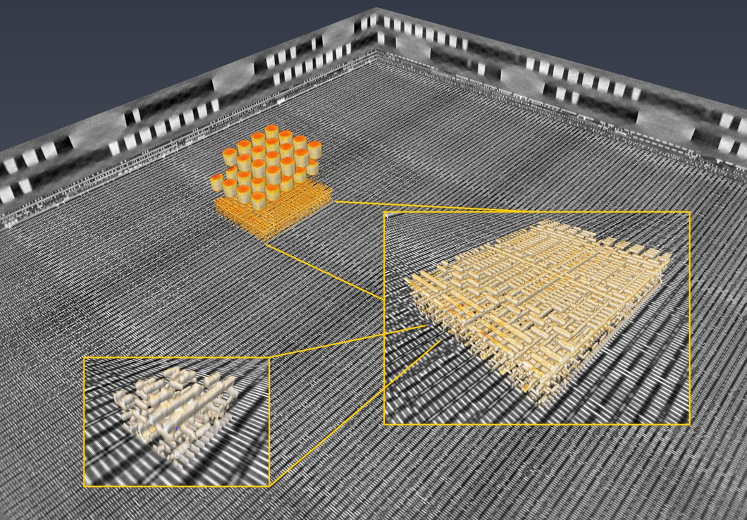
Researchers from the University of Southern California, as well as the Swiss Federal Institutes of Technology and the Paul Scherrer Institute (PSI) in Switzerland have invented a new non-destructive technique to reverse engineer an entire chip without damaging it. The technique is called ptychographic X-ray laminography and is actually an upgrade to a technique called ptychographic computed tomography that the researchers first announced in 2017.
What Is Ptychographic X-ray Laminography?
According to the researchers, the ptychographic X-ray laminography is the only non-destructive technique that doesn’t require cutting up the chip. The technology allows for the imaging of the entire chip and to zoom into specific areas.
In comparison, existing reverse engineering technologies require taking a chip apart layer by layer and mapping them using different imaging techniques such as optical microscopy for the larger elements to electron microscopy for the smallest ones.
Article continues belowTalking about the ptychographic X-ray laminography technology, professor of electrical and computer engineering at University of Southern California Anthony F. J. Levi, told IEEE Spectrum that:
“It’s the only approach to non-destructive reverse engineering of electronic chips—[and] not just reverse engineering but assurance that chips are manufactured according to design. You can identify the foundry, aspects of the design, who did the design. It’s like a fingerprint.”
The researchers’ prior technique had to use too many x-rays, which wouldn’t result in a very clear image of the chip. The new technique can shoot the x-rays at an angle (61 degrees to be exact) but still loses some chip information.
However, these gaps can be filled by knowing what type of interconnects are supposed to be in those specific locations. Knowing the design rules of the chip before starting the process can allow for the use of even fewer photons, so the final image should be even more clear with less information loss.
Get Tom's Hardware's best news and in-depth reviews, straight to your inbox.
What Are the Implications For This New Technology?
The technology could have all sorts of implications, such as allowing integrated circuit designers to verify if a chip matches its promised specifications.
Another benefit could be that having a cheaper way to reverse engineer chips would allow new entrants in the chip market to study the incumbents’ designs and then compete more effectively in the market. Reverse engineering is generally not illegal, but the new technology may not exactly make the chip incumbents happy that it exists.
Furthermore, easier and cheaper ways to reverse engineer chips would also allow for the finding of more security flaws in hardware. Intel may not be able to catch a break anytime soon, even with the new hardware mitigations it’s researching.
Using such technology, governments that don’t trust chipmakers from other countries could also more easily discover if a chip has a hidden backdoor in it, or not. There was recently a large controversy started by a Bloomberg report about a possible backdoor in Supermicro’s motherboards.
The story was controversial because many experts wanted to see more evidence that what Bloomberg was reporting was real. If a non-destructive reverse engineering technology would have been available and easily accessible by many of the chipmakers’ own customers or even security researchers, it would have been easier to get to the bottom of the story and find out if the allegation was true or not.
Lucian Armasu is a Contributing Writer for Tom's Hardware US. He covers software news and the issues surrounding privacy and security.
-
martel80 This is not so simple. After getting the complete transistor + interconnect layout, you would need some kind of synthesis tool in order to guess (interpret) what part of chip serves what high-level function.Reply -
mortemas Hmmm, maybe shielding the internals of the chip with a layer of Pb would be a good countermeasureReply -
bit_user Reply
Some chips are allegedly bonded to their heatspreader with solder. However, I don't know if that ever contains lead, or how much lead you'd actually need to effectively block these x-rays.mortemas said:Hmmm, maybe shielding the internals of the chip with a layer of Pb would be a good countermeasure
I wonder if this can be used for troubleshooting, or to measure things like metal migration.

![Ptychographic X-ray laminography could reveal the metal parts of an inverter [right]. Showing a good match for the circuit [middle, left]. Image: PSI](https://cdn.mos.cms.futurecdn.net/8v82x5R3czg2MKFfxcGvaZ.jpg)