Hot Chips 2017: A Closer Look At Google's TPU v2
Get Tom's Hardware's best news and in-depth reviews, straight to your inbox.
You are now subscribed
Your newsletter sign-up was successful
Google's Cliff Young shared details about the company's original TPU (Tensor Processor Unit) at Hot Chips 2017, but most importantly, the company also revealed more details about the Cloud TPU, otherwise known as TPU v2, during its keynote.
News that Google had designed its own ASIC in a skunkworks-class project took the internet by storm last year. Surprisingly, the secretive Google already had TPUs deployed in its data centers for a year before it disclosed its AI initiative.
Google resorted to building its own ASICs due to frustration with the slowing pace of processor development. Moore's Law is either expiring or not, depending on who you ask, but Google firmly believes that it is either in a slowdown or near retirement. Dennard scaling, which dictates that transistors maintain the same power density as they shrink, already expired around 2006 due to increased current leakage. That means we no longer see massive clock frequency increases with newer processors, which certainly doesn't set the stage for explosive generational improvements.
Article continues belowLarge price reductions and massive performance gains may be off the shelf, but Google's user base continues to grow daily. As such, Google stepped into the processor design realm to avoid growing its data center footprint.
The first generation TPU, which we'll cover shortly, only supports 8-bit integer operations. That means it can perform inference, but training is out of reach. Google has already moved onto its TPU v2, which can run both training and inference workloads. The new design is already chugging away in the company's data centers.
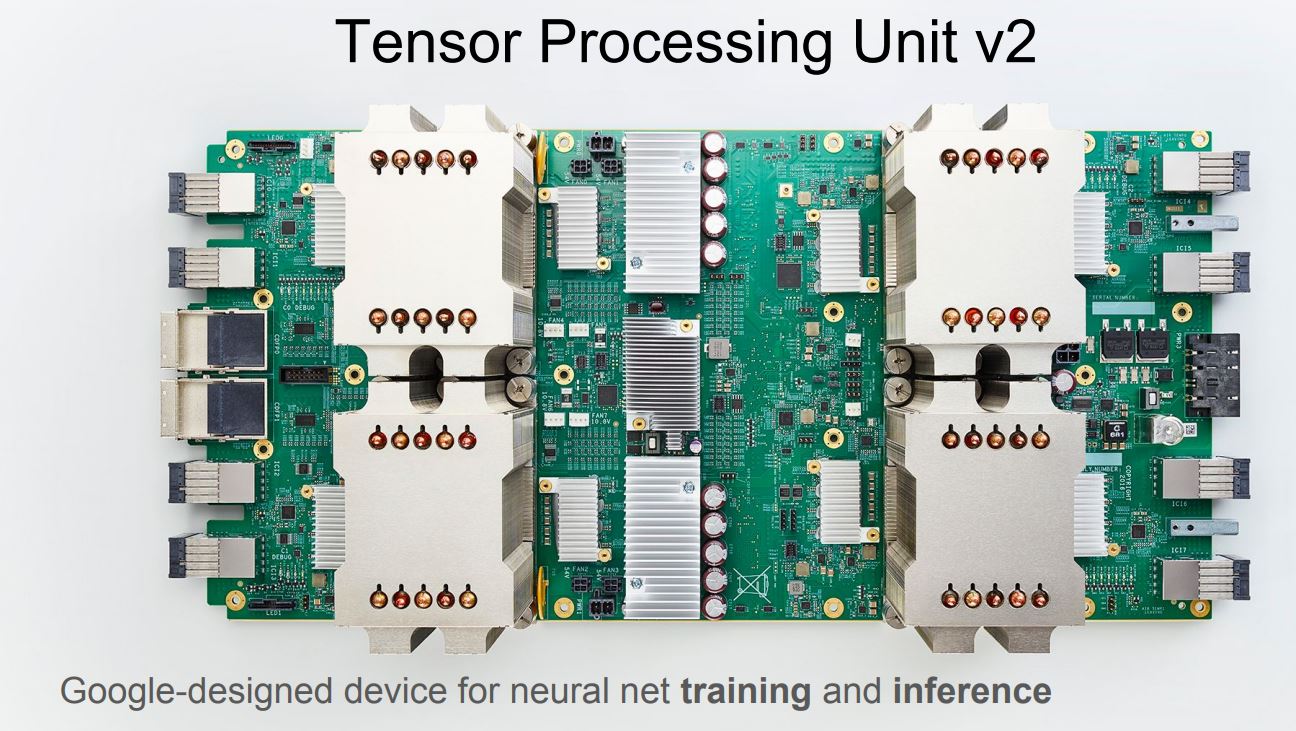
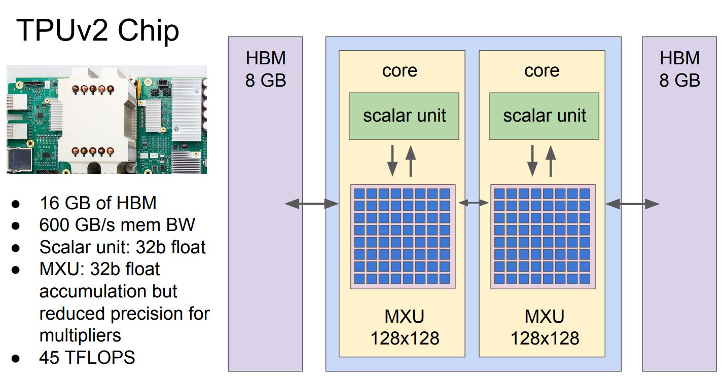

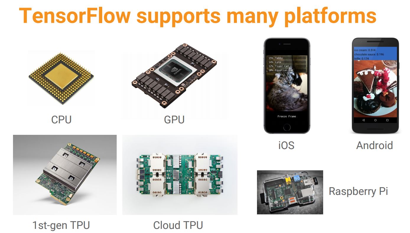
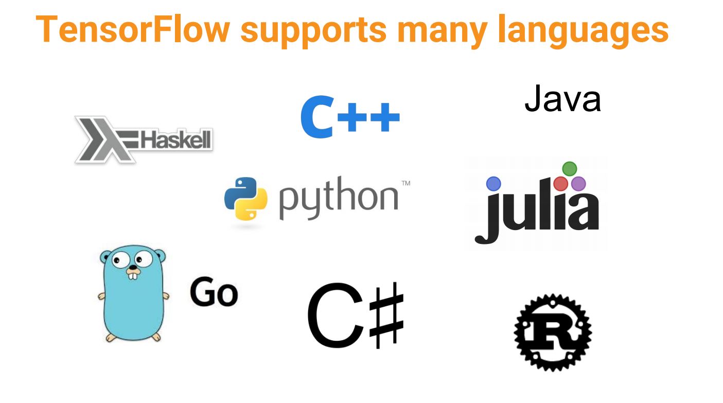
The original TPU sported a single core with a 256x256x8b Mixed Multiply Unit (MXU), but Google's Cloud TPU features dual cores with one 128x128x32b MXU apiece. Both the scalar unit and the MXU can handle 32-bit floating point operations, and each chip provides up to 45 TFLOPS. Each core is connected to the neighboring core along with 8GB of HBM (High Bandwidth Memory) that provides 600 GBps of bandwidth.
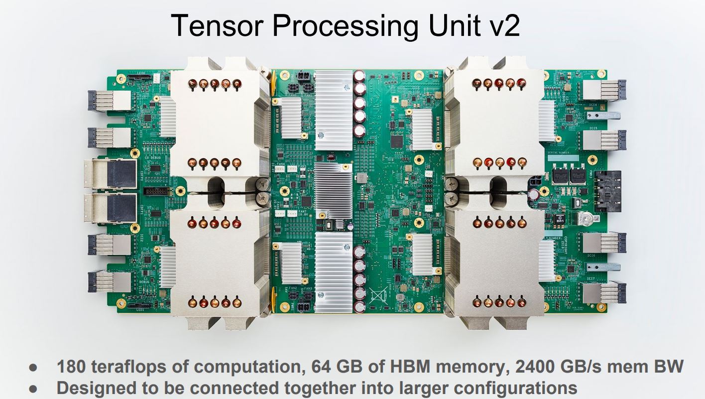
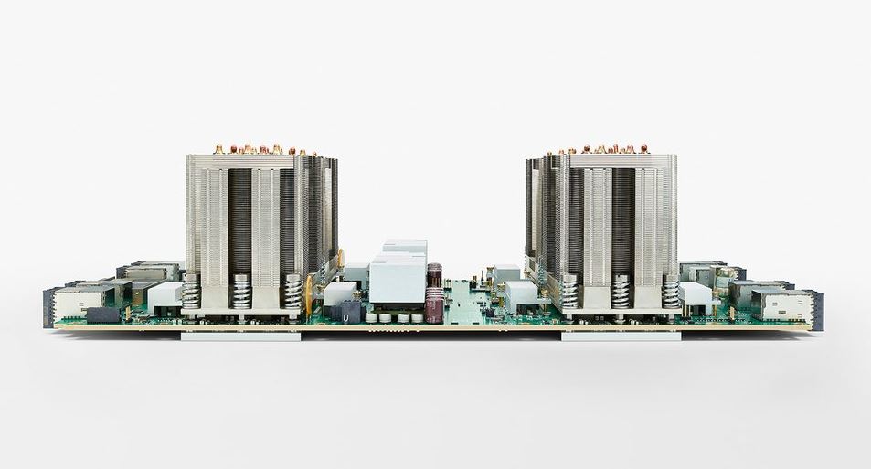
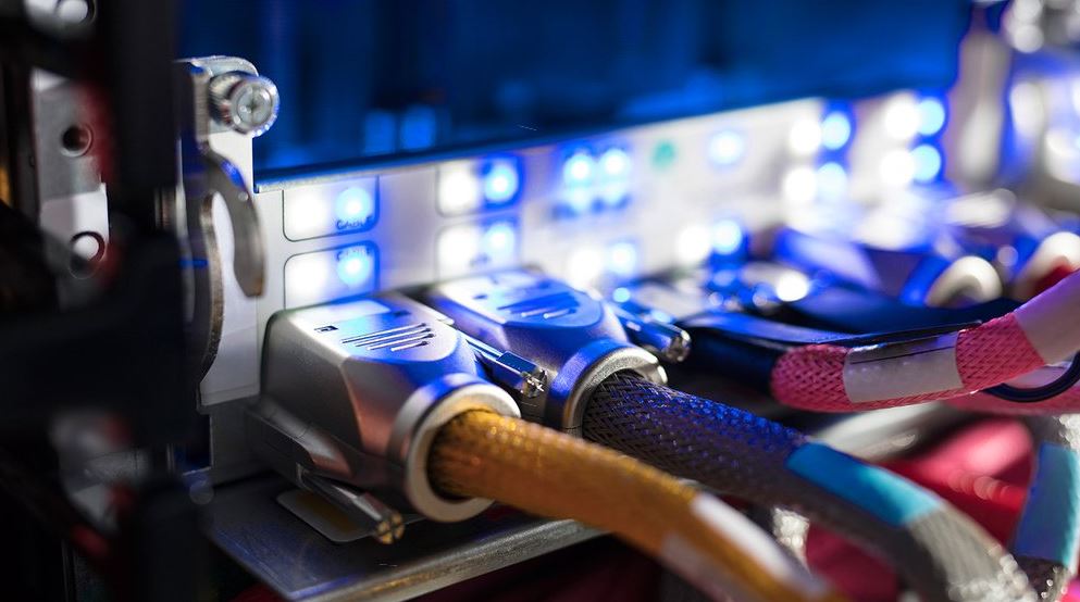
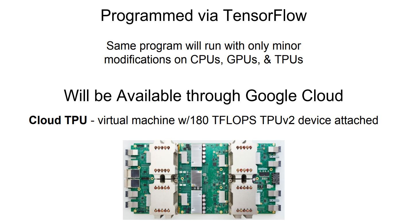
The ASICs ride on a motherboard with large heatsinks that imply hefty power consumption, but Google hasn't disclosed the official power specifications. There are also eight networking connectors on the edge of the board, widely thought to be Intel's Omni-Path and IBM's BlueLink.
Get Tom's Hardware's best news and in-depth reviews, straight to your inbox.
Out of necessity, Google designed its first generation TPU to fit into 3.5" drive bays in existing servers. The Cloud TPU uses a more traditional design that consists of four ASICs on a single motherboard with a hefty 64GB of HBM that provides 2,400 GBps of memory bandwidth. The combination powers up to 180 TFLOPS per board—but Google has larger ambitions.
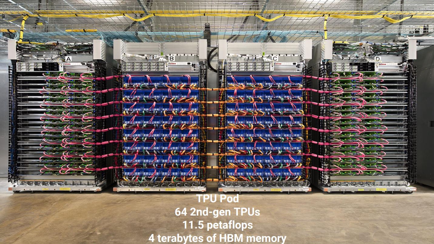
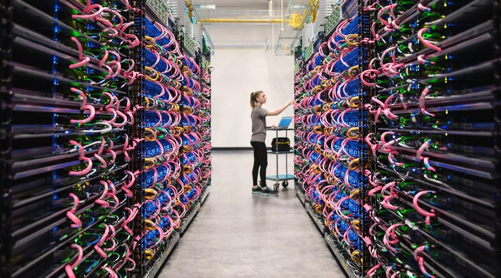
The company deploys 64 Cloud TPUs into a single "pod" that generates up to 11.5 petaFLOPS of compute and wields 4 TB of HBM. Google hasn't disclosed how many pods are currently active, but it has posted pictures of three deployments. If you wonder why HBM is in short supply, the Cloud TPUs might be part of the answer.
Google's only used the original TPUs internally, but the company is offering Cloud TPU services to the public this year through its Google Cloud Platform. Each Virtual Machine instance will come with one TPU attached. The company is also donating a thousand of the units to top researchers. Cloud TPUs are programmable with TensorFlow, which should help speed adoption.
Google hasn't provided efficiency measurements yet, but it does claim the processors offer 50% more performance than the first-generation model. We expect more details to trickle out over the coming months.
First Generation TPUs
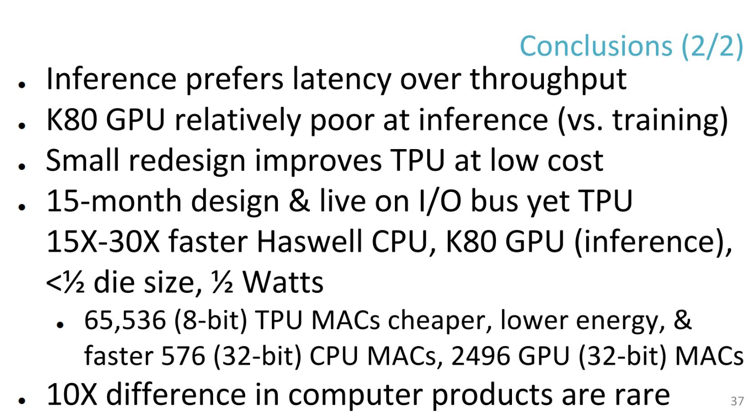
Google also unveiled a few more interesting details about its first-generation TPUs. Google's first generation TPU, now a year and a half old, was designed to perform one task—inference. The team began the design process in 2013 with the theme of "go fast and run with scissors," and fourteen months later, the TPU made its debut in Google's data centers.
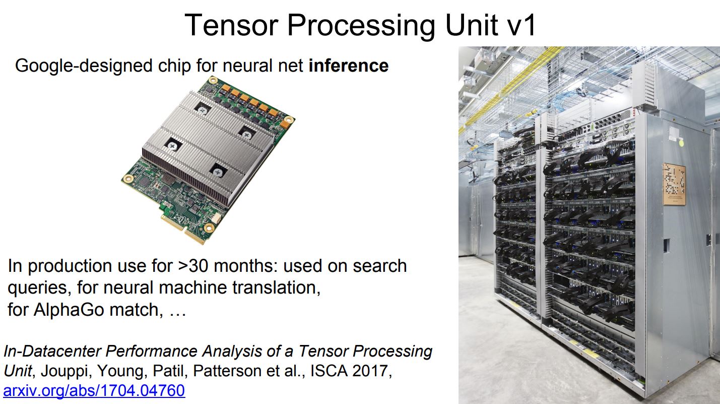
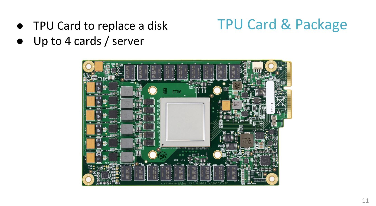
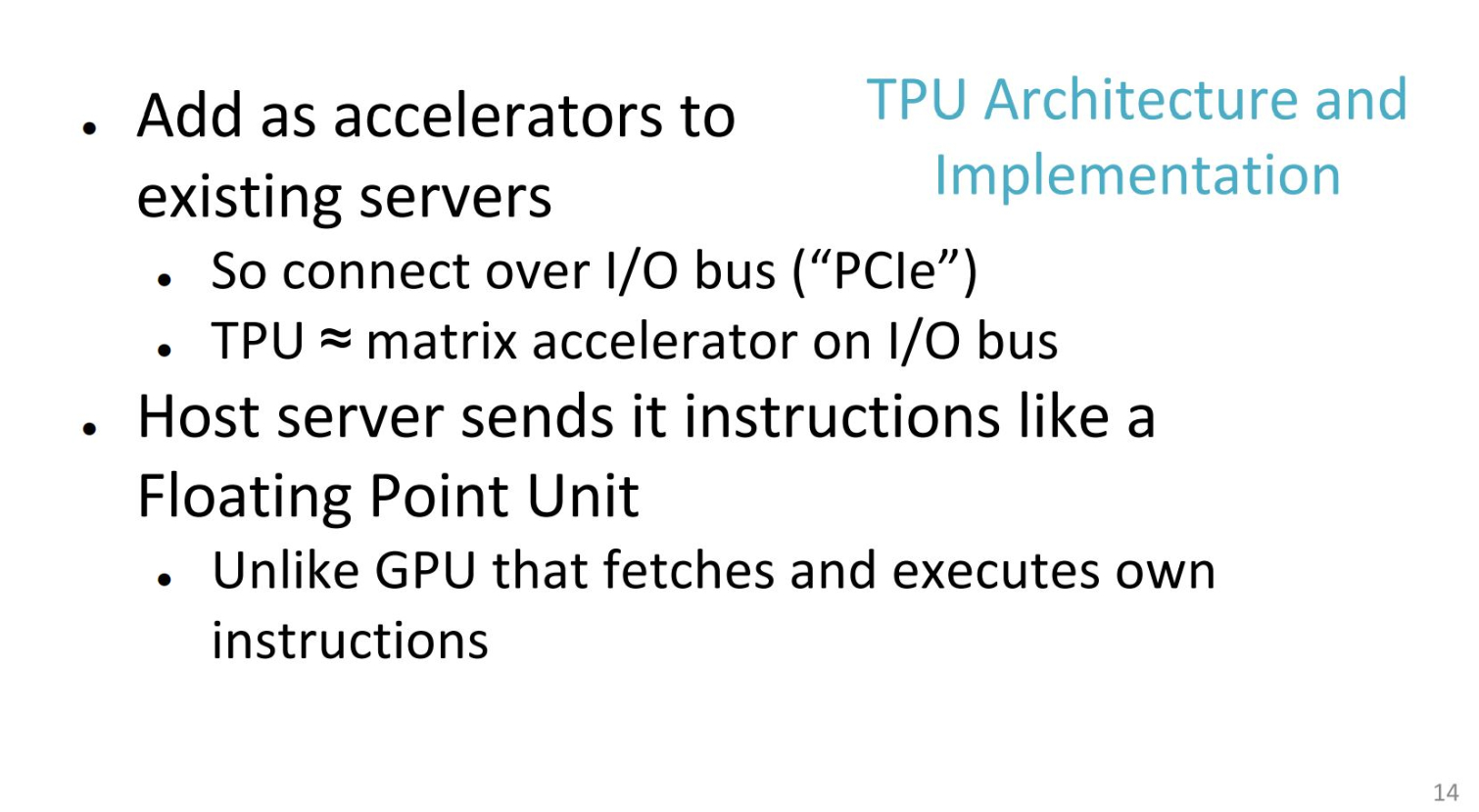
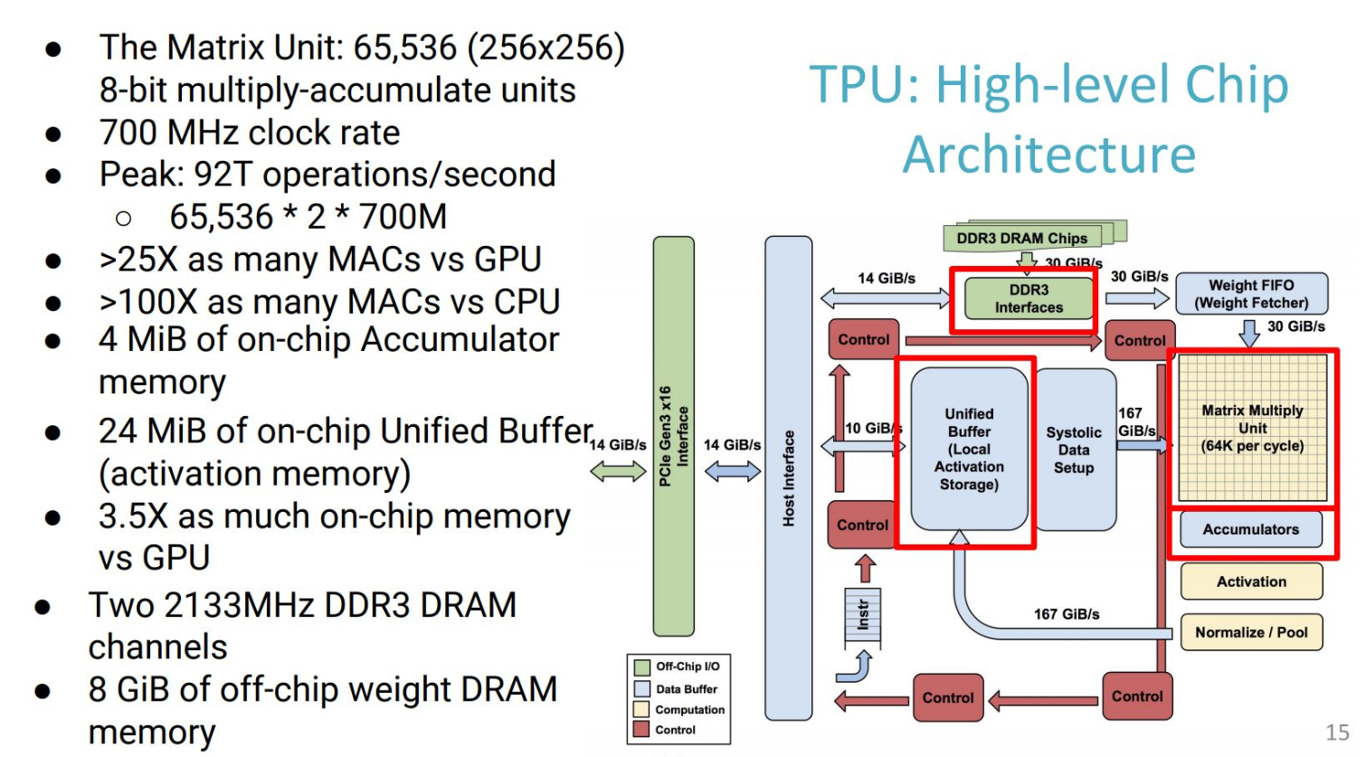
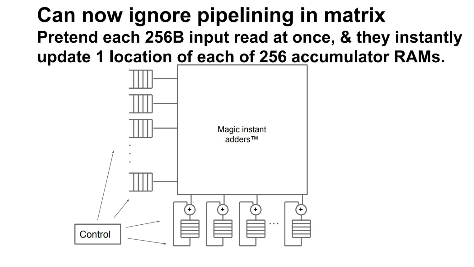
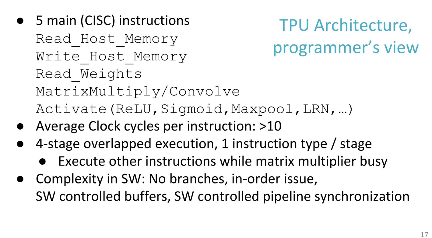
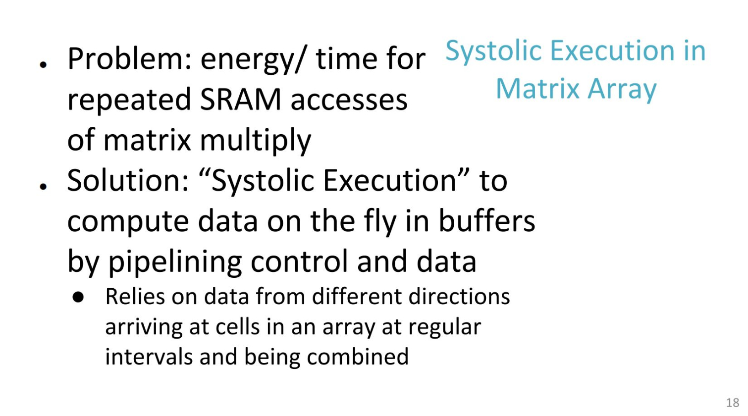
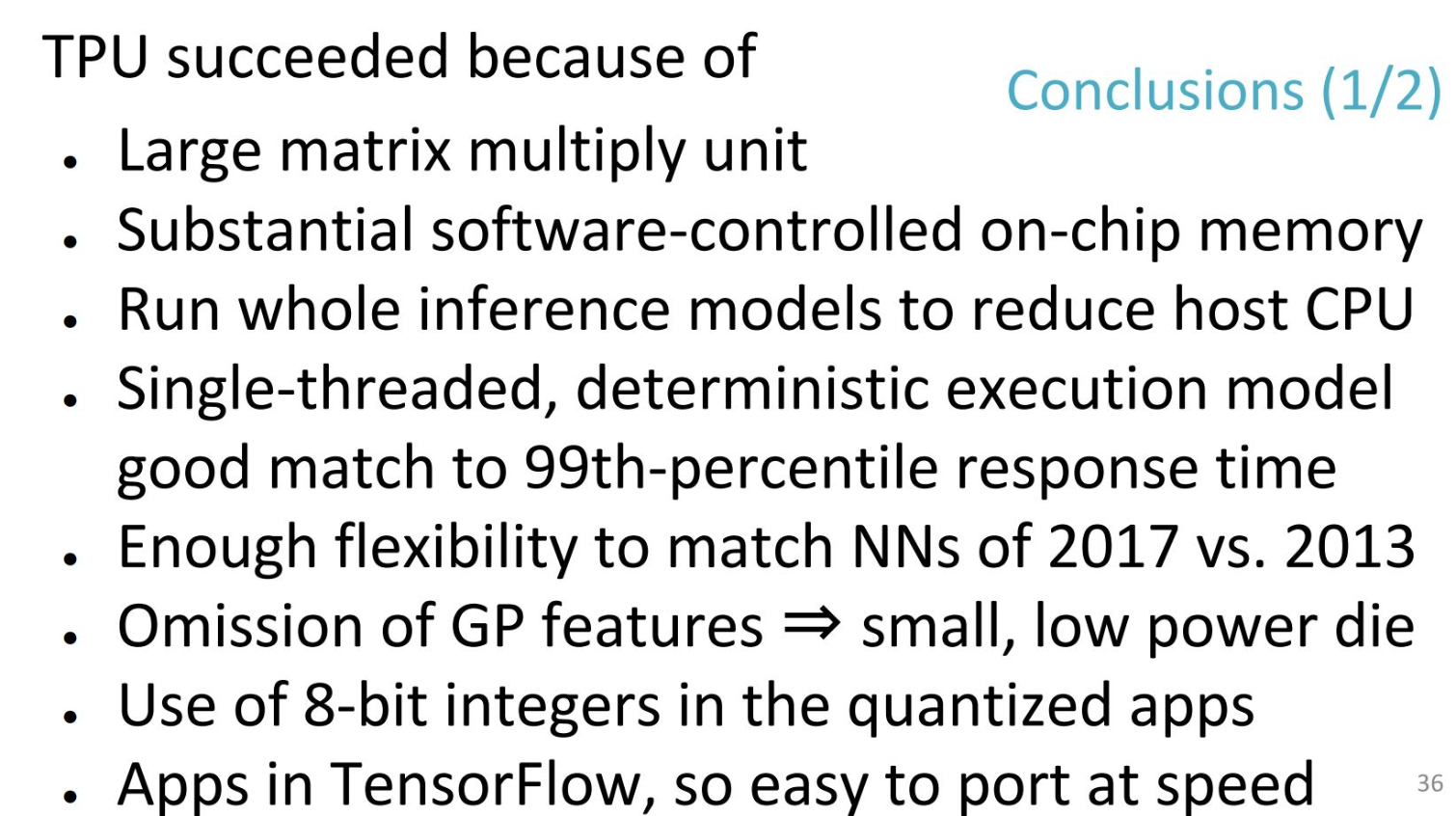
The engineers strove to maintain backward compatibility with existing infrastructure, so they designed the TPU to fit into a standard 3.5" server HDD bay and connect via a custom PCIe 3.0 x16 connector to a backplane. Google also has AIC (Add In Card) form factor models that slot in like a standard GPU. Google can pack in four TPUs per server for the most compute-intensive workloads. A 28nm ASIC sets at the heart of the device. Google doesn't reveal its foundry partner, but we know the ASIC consumes 40W under load.
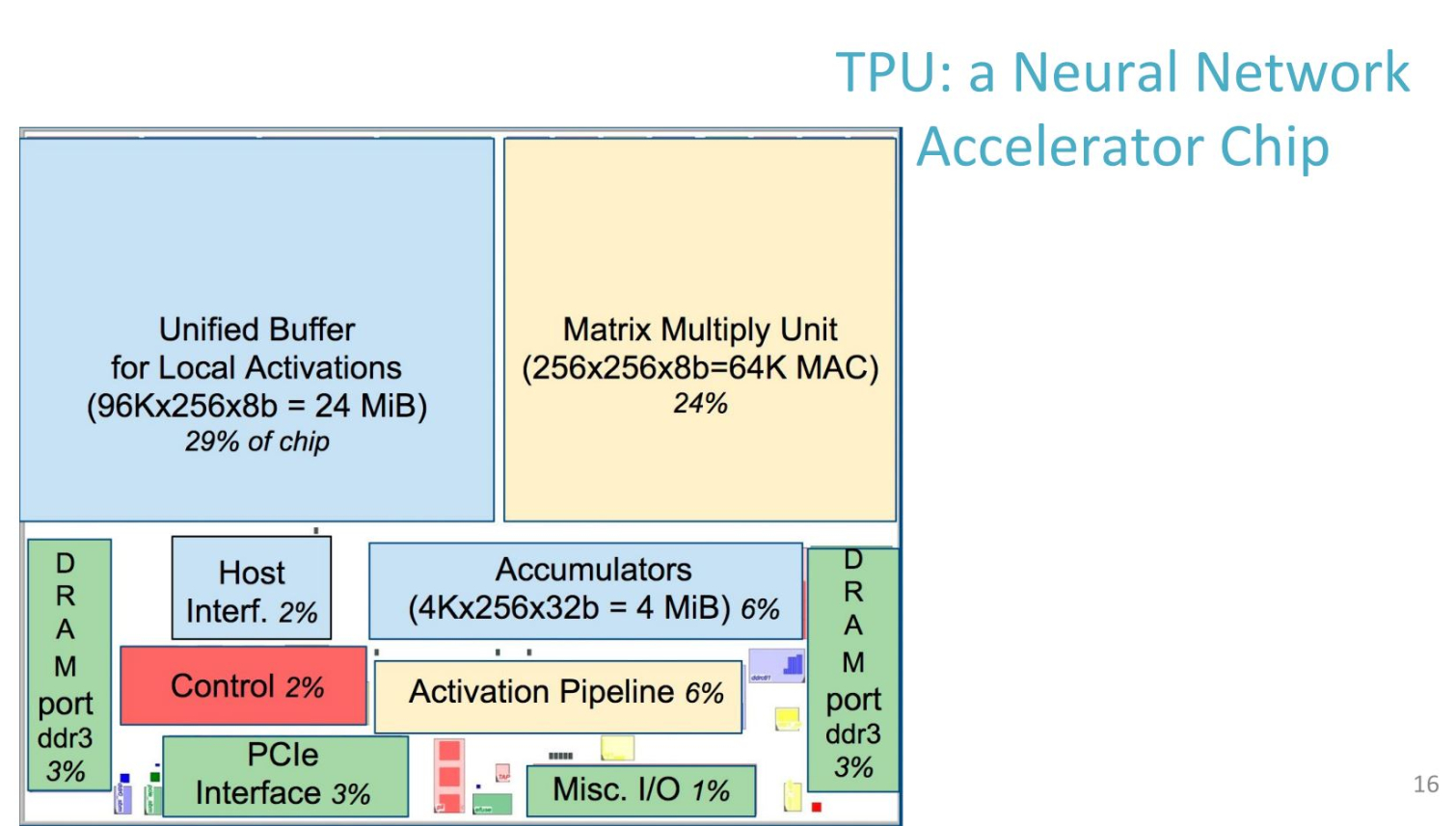
Google focused on minimizing the amount of code on the TPU, so it doesn't have its own branch processor. Instead, the host feeds it instructions. The ASIC runs at 700MHz. Its 256x256 Matrix Multiply Unit (MXU) processes hundreds of thousands of operations per clock cycle, far outweighing scalar and vector processors. The unified buffer consists of 24MB of SRAM that function as registers. The fifth slide outlines the chip design, with memory units in blue and compute units in yellow. The TPU only supports 11 instructions, but only five are used to execute workloads.
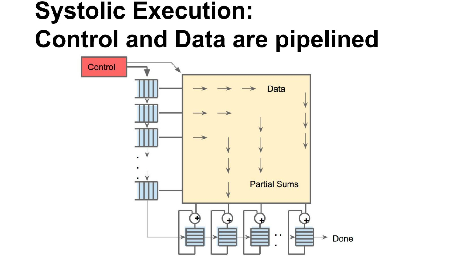
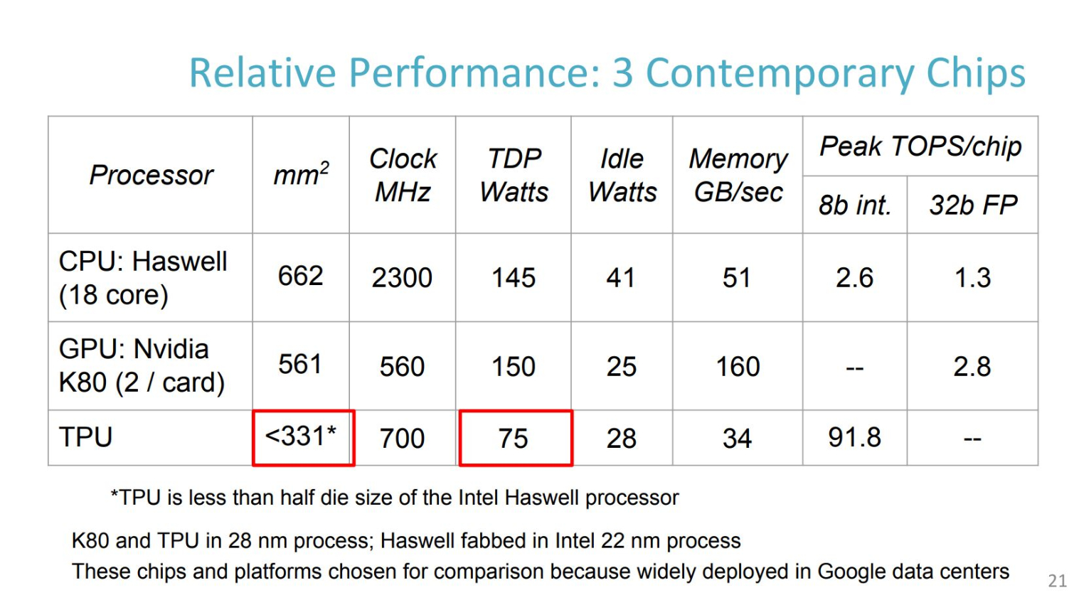
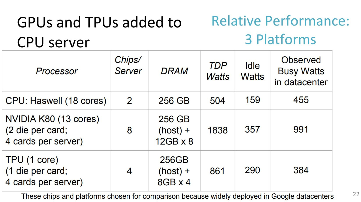
The TPU die area is less than half that of the Haswell eighteen core CPU and Nvidia's Tesla K80 GPUs (the preferred solutions at the time), which yields a much lower rating of 75W, compared to 145W and 150W, respectively. Idle power consumption is higher than a GPU, but lower than a CPU. Notably, the TPU memory bandwidth is far lower than the competing CPU and GPU, but it still manages to provide superior peak TOPS (Trillions of Operations Per Second) throughput. Google published an article that dives further into the systolic array, head there for further detail.
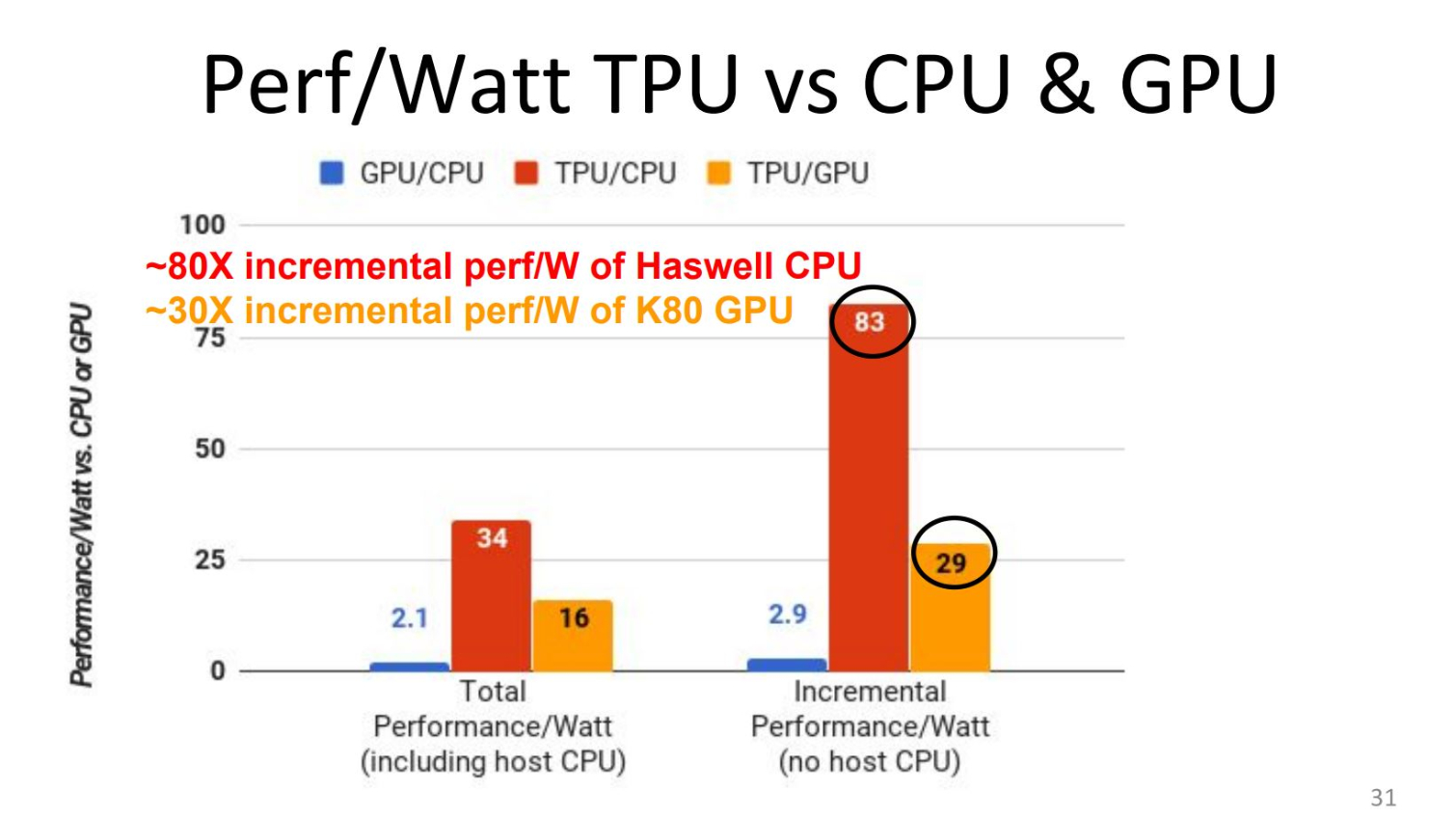
Google claims the TPU provides 15x more performance per watt than a Haswell CPU, and up to 30x more than Nvidia's K80 GPU. These performance gains reportedly allowed Google to save the expense of nearly doubling its 15 data centers.
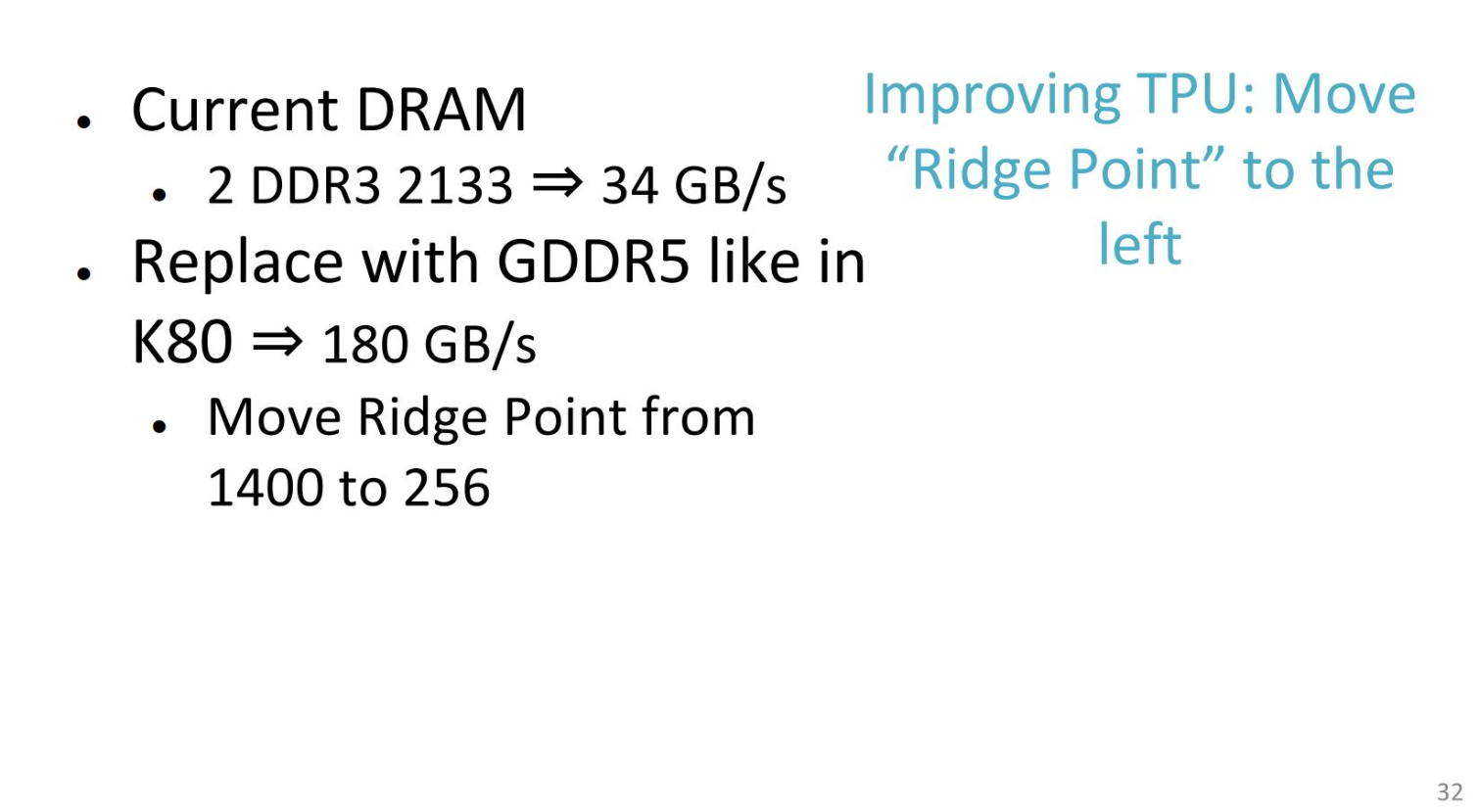
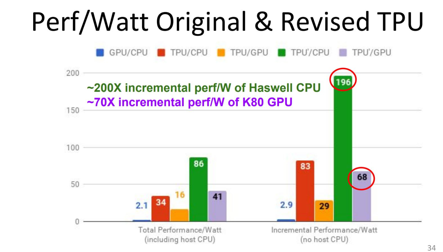
Memory bandwidth ended up being the primary limitation to the TPU design -- if Google had outfitted the processor with GDDR5, it could have ended up with far more performance per watt. The company addressed the memory deficiency with HBM memory on the second-generation Cloud TPUs.
Thoughts
Google's initial TPU posed little threat to the incumbents, such as Intel, Nvidia, and AMD, because the company only used the ASICs for its own internal operations. That might have reduced processor sales to Google, but it did little to threaten the broader AI market. Now that Google is opening up the Cloud TPU to the masses via its cloud platform, it's clear the company has wider ambitions. We expect Google's Cloud TPU, which comes online to the public later this year, could have a transformative impact on the broader market.

Paul Alcorn is the Editor-in-Chief for Tom's Hardware US. He also writes news and reviews on CPUs, storage, and enterprise hardware.
-
bit_user ReplyIf you wonder why HBM is in short supply, the Cloud TPUs might be part of the answer.
I had this thought, as it seems AMD was caught off-guard by higher-than-expected HBM2 prices. So, do we know it's definitely HBM and not HBM2? -
bit_user It's also rather disingenuous to compare TPU2 to Kepler. Based on when it came online, they should've compared it to Pascal.Reply
However, the more interesting comparison is between the TPU and GP102. The latter claims to achieve 45.5 8-bit TOPS, with a nominal TDP of 250 W. So, the original TPU still has 6.7x better efficiency.
Anyway, I wonder why the TPU2 with 32-bit, while everyone else is trying to do inferencing with 16-bit floats. -
TadashiTG Eh, I think by now when someone says "HBM" people should know they are referring to HBM2. The first generation is probably not very useful anymore, and could be out of production altogether.Reply
You can also tell by the capacity being larger than 4GB.