WD Touts 3D NAND That's 60% Faster and 50% Higher Capacity
Western Digital this week gave a sneak peek at its BiCS 3D NAND roadmap for the next few years. As expected, the company and its partner Kioxia will continue to introduce new generations of its BiCS memory increasing per-device capacity and lowering per-bit costs.
Furthermore, the company is developing its BiCS+ 3D NAND that will substantially increase performance and density compared to regular BiCS memory to enable ultra-high-capacity SSDs with extreme performance.
162-Layer BiCS6 Incoming
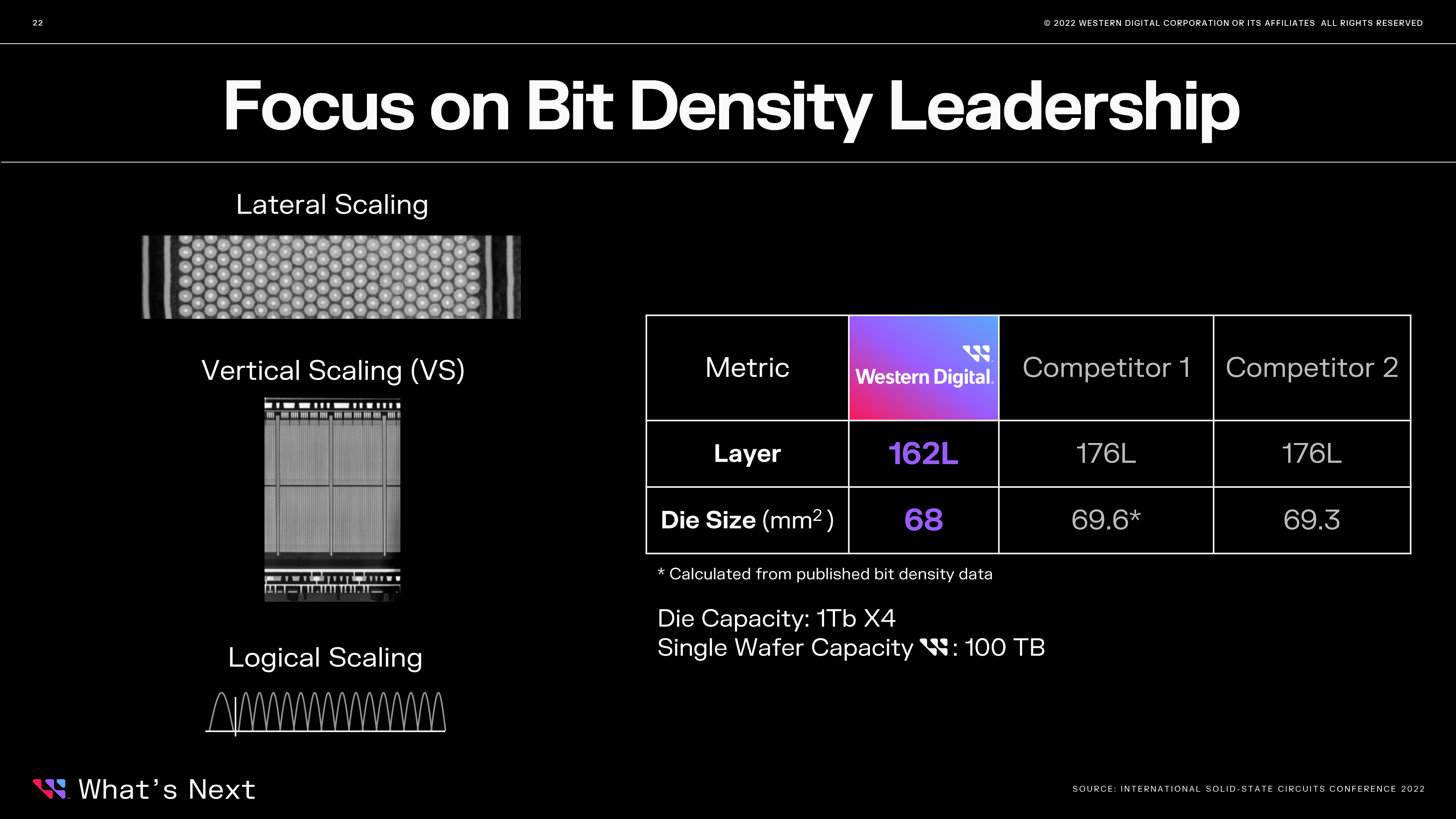
The company's next step is introduction of its 6th Generation BiCS memory that will feature 162 active layers and will enable 1 Tb QLC 3D NAND memory devices with a die size of 68 mm^2. The new generation Western Digital's 3D NAND will also feature a faster I/O interface and a 60MB/s program speed, which will significantly increase performance of next-generation SSDs, particularly those mainstream drives with a PCIe 5.0 interface.
While 162 layers may not look as impressive as the 176 layers touted by other makers, Western Digital's die size will be smaller when compared to the die sizes of competitors because the company will shrink memory cell size by using a new material. As a result, the company hopes that its BiCS6 1Tb 3D QLC ICs will be easier and cheaper to produce, which will enable it to build cheaper storage devices that compete with the best SSDs on performance and pricing.
Mass production of BiCS6 3D NAND memory in QLC and TLC configuration is set to start in late 2022 (Q2 of WDC's FY2023). BiCS6 3D NAND chips will be used for a broad array of applications starting from inexpensive USB drives and scaling all the way to high-priced high-capacity SSDs.
200+ Layer BiCS+ Incoming
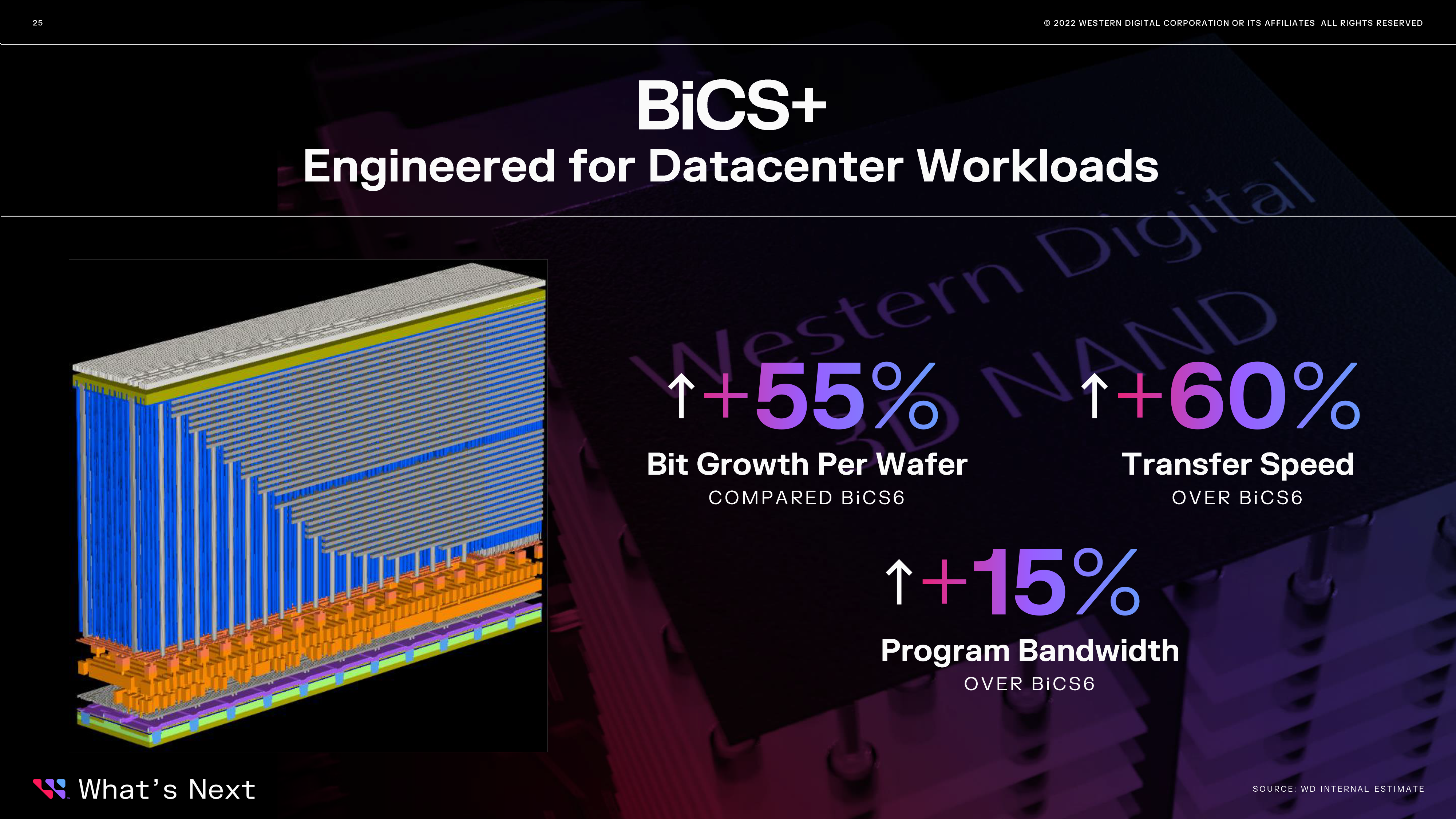
Meanwhile, specifically for datacenter workloads that need both high capacity and high performance, Western Digital intends to introduce BiCS+ memory that was designed for datacenters from the ground up.
The company claims that when compared to BiCS6, BiCS+ will provide a 55% bit growth per wafer thanks to 200+ layers, an up to 60% higher transfer speed (i.e., will use a faster interface and/or 8/16-plane architecture for higher parallelism), and a 15% higher program bandwidth (i.e., higher write speed). At present BICS+ is set to arrive sometimes towards 2024.
Get Tom's Hardware's best news and in-depth reviews, straight to your inbox.

"This is engineered for the datacenter workloads and you can see […] a 55% bit growth rate per wafer when we go from BiCS6 to this node, a 60% increase in I/O speed, and the program bandwidth, I just talked about which we hold the world record at 60MB/s, on that cell we are pushing that up even further by another 15%," said Siva Sivaram, president of technology and strategy at Western Digital. "By the time this is developed and ramping, this will be a quantum leap in the performance of NAND."
While Western Digital did not outline its exact BiCS+ plans, we would expect this new type of memory to allow the company to produce high-capacity datacenter SSDs in standard form-factors without using tricky packaging or very complex controllers. It should also be noted that BiCS+ is indeed aimed specifically at datacenter drives as for regular SSDs the company intends to offer 200+ layers memory currently referred to as BiCS-Y.
Speaking of datacenter SSDs, it is interesting to note than unlike its partner Kioxia, Western Digital no longer talks about 3D NAND-based storage class memory (SCM) competing against both Intel's Optane and Kioxia's XL NAND. The company once mentioned its low-latency flash (LLF) NAND memory for SCM applications in 2019, but since then it has provided no updates.
In theory, high-density 3D NAND can be used in single-level cell (SLC) mode to address applications that need high performance, low latency, high reliability, and great data retention. Meanwhile, we are not sure whether media designed for BiCS+ components can be used in this mode for the aforementioned applications.
Technologies In Development
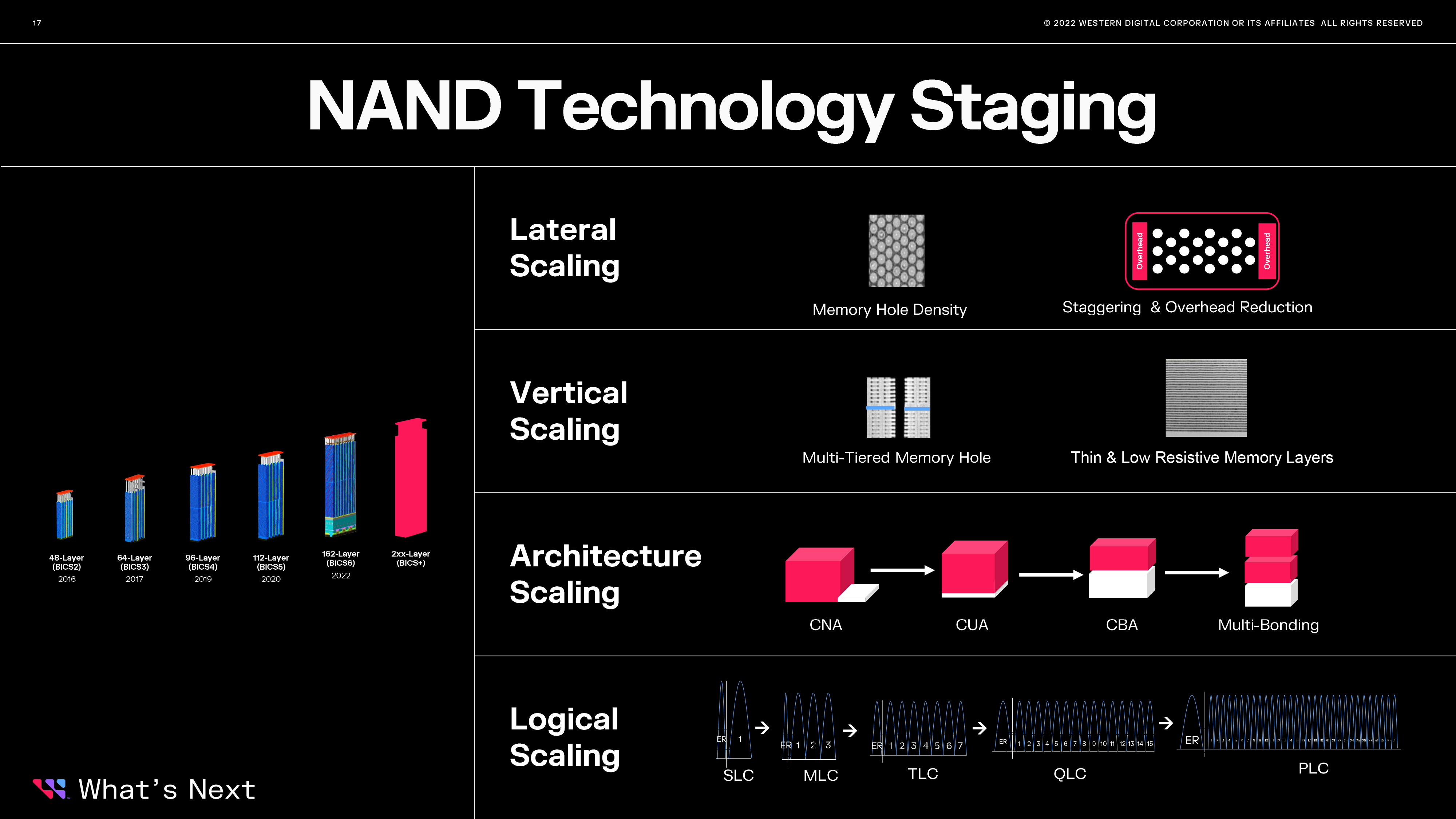
There are many ways to increase capacity of a 3D NAND memory device, including increasing the number of bits stored per cell (MLC, TCL, QLC, etc.), making a cell smaller, adding more vertical layers, or increasing the number of layers by bonding together two 3D NAND wafers. All of these technologies were used in the past and will continue to be used in the future.
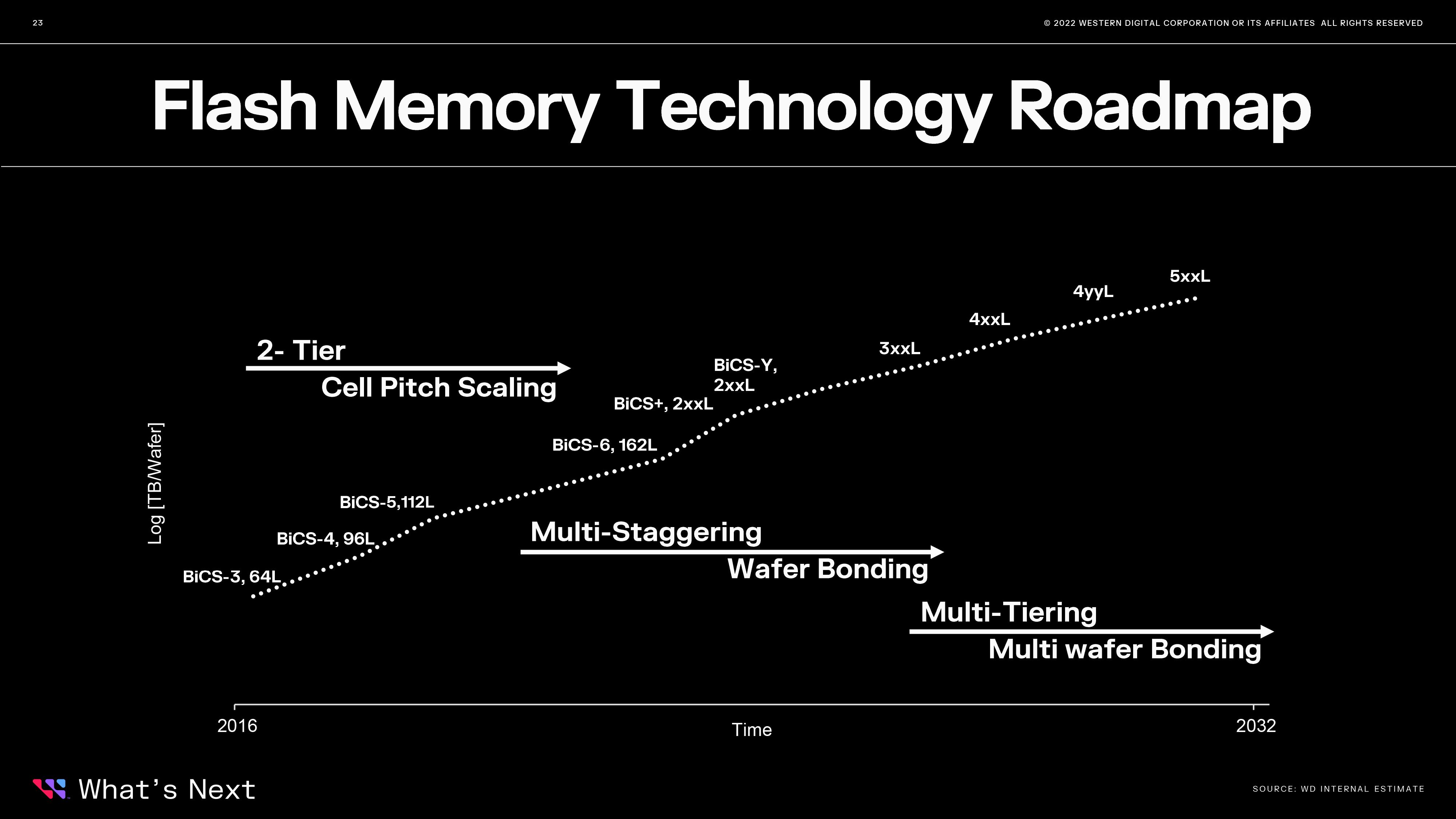
Eventually, we are going to see 3D NAND memory ICs with over 500 layers made by bonding several wafers and using other advanced techniques, but this is not going to happen before the year 2030 or so, according to Western Digital.
"You can see [that] over the next 10+ years we have a good roadmap that technology is being developed and staged to go all the way up to 500 plus layers," said Sivaram "We started with 3D NAND, two tiers, we started the scale the cell pitch, we started putting more staggers between overhead lines, we probably will introduce wafer bonding, we will do multi tearing, multi wafer bonding. These technologies are already in the works being in place so that we can introduce them at the right node […]."
Being among the world's largest makers of 3D NAND memory that produce over 500,000 of 3D NAND wafers per month, Kioxia and Western Digital are naturally studying and developing a host of technologies that will enable them to scale capacity of their 3D NAND devices going forward.
As usual, makers of 3D NAND are extremely reluctant to share details about their future nodes (and even current nodes, actually) for competitive reasons, so we do not know what capability will enable BiCS7 or BiCS8 nodes.
PLC Mentioned. Kind Of
Western Digital's president of technology and strategy barely mentioned penta-level cell (PLC) 3D NAND memory (which packs in five bits per cell using 32 distinct voltage levels) verbally, yet it is noteworthy that his his presentation did contain a reference to PLC 3D NAND as one of the next technologies.
Last year, Sivaram downplayed advantages of PLC 3D NAND citing complications with controllers and challenges like cell-to-cell interference and temperatures. For now, PLC 3D NAND may not be on the table for Western Digital, but the very mention of this technology indicates that the company is at least considering it, albeit not for the BiCS6 generation.

Anton Shilov is a contributing writer at Tom’s Hardware. Over the past couple of decades, he has covered everything from CPUs and GPUs to supercomputers and from modern process technologies and latest fab tools to high-tech industry trends.


