Introduction
Here are the specs of the latest Pentium Pro Chipset, just released from VIA. This chipset has the ability to defeat Intel for the first time since they released their Triton chipset. At present there is NO OTHER PPro chipset around that offers even slightly as much as this high performance chipset. If a high quality motherboard with that chipset should be out soon, I might even change my mind and get a PPro myself.
Actually I just found the first motherboard which uses the Apollo P6, it's the FIC PA-6010. Go and have a look! As soon as there's another new one out there, I'll tell you.
- High Integration
- VT82C685 system controllerVT82C687 data bufferVT82C586 PCI to ISA bridgeSix TTLs for a complete main board implementation
- Flexible CPU Interface
- 64 bit Pentium-ProTM CPU interfaceCPU external bus speed up to 66 MHzSupports Pentium-ProTM CPU multi-phase bus protocol for split transactionsSupports four level deep in-order-queue and deferred transactionSupports APICTM multiprocessor protocolGTL+TM bus driver and receiver compatible with Intel specification
- Fast DRAM Controller
- Sixteen level (quadwords) of CPU to DRAM write buffersSixteen level (quadwords) of DRAM to CPU read buffersFast Page Mode/EDO/Burst EDO/Synchronous-DRAM support in a mixed combinationMixed 1M/2M/4M/8M/16MxN DRAMsSupports 2-way bank-interleaving of 16 MB SDRAMSupports 2-way and 4-way bank-interleaving of 64 MB SDRAM6 banks up to 1 GB DRAMsFlexible row and column addressesOptional bank-by-bank ECC and parity generation, detection, and correction capabilityECC with 1 bit error correction and multi-bit error detection capability3.3v and 5v DRAM without external buffersBurst read and write operation5-1-1-1-1-1-1-1 back-to-back Burst EDO and Synchronous DRAM transfer at 66 MHz532 MB/s peak transfer rate for Burst EDO and Synchronous DRAMs at 66 MHz266 MB/s peak transfer rate for EDO DRAMs at 66 MHzBIOS shadow at 16 kB incrementSystem management memory remappingDecoupled and burst DRAM refresh with staggered RAS timingProgrammable refresh rate, CAS-before-RAS refresh and refresh on populated banks only
- Intelligent PCI Bus Controller
- 32 bit 3.3/5v PCI interfaceSynchronous divide-by-two PCI bus interfacePCI master snoop ahead and snoop filteringConcurrent PCI master/CPU/IDE operationsSynchronous Bus to CPU clock with divide-by-two from the CPU clockAutomatic detection of data streaming burst cycles from CPU to the PCI busSixteen levels (double-words) of CPU to PCI posted write buffersByte merging in the write buffers to reduce the number of PCI cycles and to create further PCI bursting possibilitiesZero wait state PCI master and slave burst transfer ratePCI to system memory data streaming up to 132 MByte/secSixteen levels (double-words) of post write buffers from PCI masters to DRAMSixteen levels (double-words) of prefetch buffers from DRAM for access by PCI mastersEnhanced PCI command optimization (MRL, MRM, MWI, etc.)Complete steerable PCI interruptsSupports CPU write-back forward to PCI master read to minimize PCI read latencySupports CPU write-back merged with PCI master post-write to minimize DRAM utilizationProvides transaction timer to fairly arbitrate between PCI mastersSupports five PCI masters in addition to PCI-ISA/IDE/USB bridgePCI-2.1 compliant
- Enhanced Master Mode PCI IDE Controller with Extension to UltraDMA-33
- Dual channel master mode PCI supporting four Enhanced IDE devicesTransfer rate up to 22 MB/sec to cover PIO mode 4 and multi-word DMA mode 2 drives and beyondExtension to UltraDMA-33 interface for up to 33 MB/sec transfer rateSixteen levels (doublewords) of prefetch and write buffersInterlaced commands between two channelsBus master programming interface for SFF-8038 rev.1.0 and Windows-95 compliantFull scatter and gather capabilitySupport ATAPI compliant devicesSupport PCI native and ATA compatibility modesComplete software driver support
- Universal Serial Bus Controller
- USB v.1.0 and Intel Universal HCI v.1.1 compatibleEighteen level (doubleword) of data FIFOs with full scatter and gather capabilitiesRoot hub and two function ports with integrated physical layer transceiversLegacy keyboard and PS2 mouse support
- Plug and Play Controller
- Dual interrupt and DMA signal steering with plug and play controlMicrosoft Windows 95TM and plug and play BIOS compliant
- Sophisticated Power Management and OnNow/ACPI Unit
- Normal, doze, sleep, suspend and conserve modesSystem event monitoring with two event classesTwo general purpose timersSixteen general purpose output portsSeven external event input ports with programmable SMI conditionPrimary and secondary interrupt differentiation for individual channelsClock throttling controlMultiple internal and external SMI sources for flexible power management modelsAPM 1.2 compliant modelsExtension to OnNow and ACPI (Advanced Configuration and Power Interface) support
- PCI to ISA Bridge
- Integrated 82C206 peripheral controllerIntegrated keyboard controller with PS2 mouse supportsIntegrated DS12885 style real time clock with extended 128 Byte CMOS RAMIntegrated USB controller with root hub and two function portsIntegrated master mode enhanced IDE controller with enhanced PCI bus commandsPCI-2.1 compliant with delay transactionFour double-word line buffer between PCI and ISA busSupports type F DMA transfersFast reset and Gate A20 operationEdge trigger or level sensitive interruptFlash EPROM, 2 MB EPROM and combined BIOS support
- Built-in Nand-tree pin scan test capability
- 0.5um mixed voltage, high speed and low power CMOS process
- 208 pin PQFP for VT82C685
- 208 pin PQFP for VT82C586
- 208 pin PQFP for VT82C687
Overview
The VT82C680 Apollo-P6 is a high performance, cost-effective and energy efficient chip set for the implementation of PCI/ISA desktop and notebook personal computer systems based on the 64 bit Intel Pentium-Pro super-scalar processors. The chipset supports multi-Pentium-Pro configuration with Intel GTL+ driver and receiver interface up to 66 MHz external CPU bus speed. The chipset supports the Pentium-Pro CPU multi-phase bus protocols for split transactions, four level deep in-order queue and deferred transactions for optimal CPU throughput.
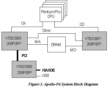
The VT82C680 chip set consists of the VT82C685 system controller, the VT82C687 data buffer and the VT82C586 PCI to ISA bridge. The VT82C680 supports six banks of DRAMs up to 1 GB. The DRAM controller supports Standard Page Mode DRAM, EDO-DRAM, Burst EDO-DRAM and Synchronous DRAM in a flexible mixed/match manner. The Burst-EDO and Synchronous DRAM allows zero wait state bursting between the DRAM and the VT82C687 data buffers at 66 MHz. The six banks of DRAM allow arbitrary mixture of 1M/2M/4M/8M/16MxN DRAMs with optional bank-by-bank ECC and parity support. The chipset supports sixteen level (quadwords) of CPU to DRAM write buffers and sixteen level (quadwords) of DRAM to CPU read buffers to maximize the CPU bus and DRAM utilization. The peak data transfer rate for the EDO and Synchronous DRAM (or Burst EDO) DRAMs is 266 MB/s and 532 MB/s, respectively.
The VT82C680 supports 3.3/5v 32 bit PCI bus with 64 bit to 32 bit data conversion. Sixteen levels (doublewords) of post write buffers are included to allow for concurrent CPU and PCI operation. Consecutive CPU addresses are converted into burst PCI cycles with Byte merging capability for optimal CPU to PCI throughput. For PCI master operation, sixteen levels (doublewords) of post write buffers and thirty-two levels (doublewords) of prefetch buffers are included for concurrent PCI bus and DRAM/cache accesses. The chipset also supports enhanced PCI bus commands such as Memory-Read-Line, Memory-Read-Multiple and Memory-Write-Invalid commands to minimize snoop overhead. In addition, the chipset supports advanced features such as snoop ahead, snoop filtering, CPU write-back forward to PCI master and CPU write-back merged with PCI post write buffers to minimize PCI master read latency and DRAM utilization. The VT82C586 PCI to ISA bridge supports four levels (doublewords) of line buffers, type F DMA transfers and delay transaction to allow efficient PCI bus utilization (PCI-2.1 compliant). The VT82C586 also includes integrated keyboard controller with PS2 mouse support, integrated DS12885 style real time clock with extended 128 Byte CMOS RAM, integrated master mode enhanced IDE controller with full scatter and gather capability and extension to 33 MB/sec UltraDMA-33 transfer rate, integrated USB interface with root hub and two function ports with built-in physical layer transceiver, and OnNow/ACPI compliant advanced configuration and power management interface. A complete main board can be implemented with only six TTLs.
The VT82C680 is ideal for high performance, high quality, high energy efficient and high integration desktop and notebook PCI/ISA computer systems.