The VIA C3 In Detail
Here's the obligatory processor diagram.
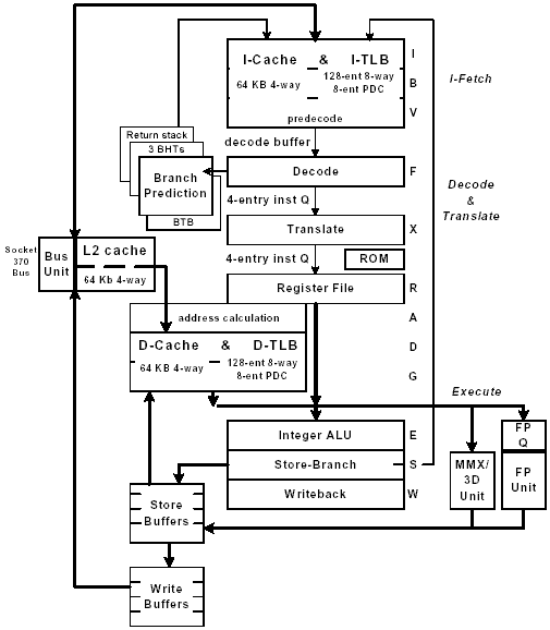
Compared to an Athlon or Pentium 4, the C3 is quite simple, which explains its benefits.
VIA tried to keep the core as small as possible, which is probably a measure to reduce heat dissipation to a minimum. As a result, the caches are comparatively small: the 64 kB data and instruction cache each (L1), plus the 64 kB L2 cache are less than the main competitors offer.
| Processor | L1 Cache | L2 Cache | FSB |
|---|---|---|---|
| Intel Celeron | 16+16 kB | 128 kB | 66/100 MHz |
| Intel Celeron | 16+16 kB | 256 kB | 100 MHz |
| Intel Pentium III | 16+16 kB | 256 kB | 100/133 MHz |
| Intel Pentium III | 16+16 kB | 512 kB | 133 MHz |
| Intel Pentium 4 | 8 kB | 256 kB | 400 MHz QDR |
| Intel Pentium 4 | 8 kB | 512 kB | 400/533 MHz QDR |
| AMD Duron | 64+64 kB | 64 kB | 200 MHz DDR |
| AMD Athlon | 64+64 kB | 256 kB | 200/266 MHz DDR |
| AMD Athlon XP | 64+64 kB | 256 kB | 266 MHz DDR |
| VIA C3 | 64+64 kB | 64 kB | 100/133 MHz |
As you can see, the C3 is equipped with quite a good amount of L1 cache, while the L2 cache is quite small.

The C3 is available in versions ranging from 800 MHz to 1 GHz, running at either 100 or 133 MHz FSB. Because the clock multiplier is locked, you should pick the right model right from the start. With only 52 mm² die size, the C3 is the smallest x86 processor available and includes both MMX and the 3DNow! Instuction set from AMD. Produced by TSMC in Taiwan in 0.13 µm, it is also one of the most advanced processors available.
For further information about the C3, please check out the C3 Ezra-T data sheet at VIA's website.


