Intel launches optical compute interconnect chiplet: Adding 4 Tbps optical connectivity to CPUs or GPUs
4 Tbps interconnects for next-generation datacenters.

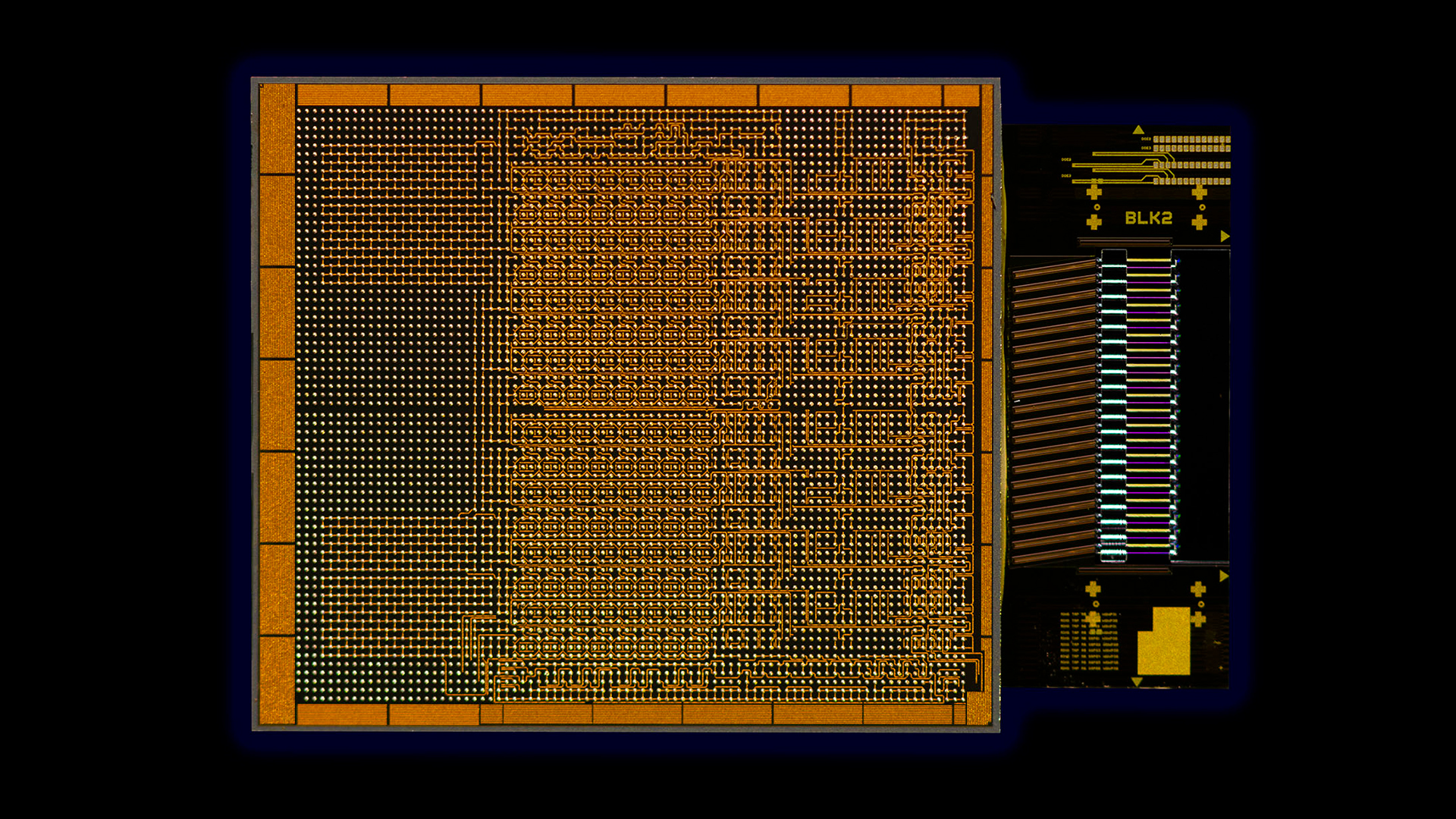
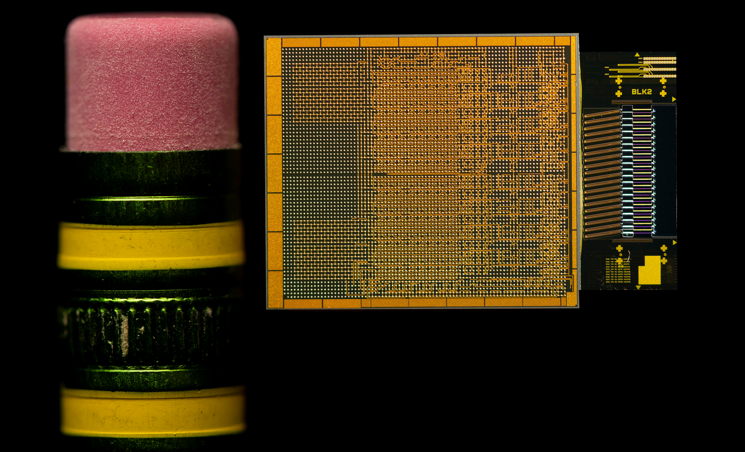
Optical interconnects are crucial for next-generation AI and HPC data centers, but adding them to CPUs and GPUs is complicated, and much of the infrastructure for mass adoption is still lacking. To that end, Intel introduced its first fully integrated optical input/output (I/O) chiplet at the Optical Fiber Communication Conference (OFC) 2024. The optical compute interconnect (OCI) chiplet can be attached to CPUs and GPUs to enable high bandwidth, low power consumption, and extended-reach I/O connectivity.
Intel's OCI chiplet is one of the industry's first fully integrated optical I/O solutions for co-packaging with compute processors. This chiplet supports 64 PCIe 5.0 channels, each transmitting at 32 GT/s in both directions, totaling 4 Tbps, over distances of up to 100 meters using fiber optics. The chiplet uses dense wavelength division multiplexing (DWDM) wavelengths and consumes only five pico-Joules per bit, significantly more energy-efficient than pluggable optical transceiver modules, which consume about 15 pico-Joules per bit, according to Intel.
This device is crucial for next-generation data centers and AI/HPC applications. It will enable high-performance connections for CPU and GPU clusters, coherent memory expansion, and resource disaggregation. These features will be handy for operating supercomputers for large-scale AI models and machine learning tasks that require tremendous data bandwidth.
Article continues belowTraditional electrical I/O systems, which rely on copper traces for connectivity, offer high bandwidth density and low power but are limited to short distances of about one meter. In contrast, Intel's optical I/O chiplet can transmit data over much longer distances with higher efficiency and lower power consumption.
The current optical I/O chiplet is largely a prototype, and Intel is collaborating with select customers to further develop and integrate this device with next-generation systems-on-chips (SoCs) and system-in-packages (SiPs).
"The ever-increasing movement of data from server to server is straining the capabilities of today’s data center infrastructure, and current solutions are rapidly approaching the practical limits of electrical I/O performance," said Thomas Liljeberg, senior director of product Management and Strategy, Integrated Photonics Solutions (IPS) Group. "However, Intel’s groundbreaking achievement empowers customers to seamlessly integrate co-packaged silicon photonics interconnect solutions into next-generation compute systems. Our OCI chiplet boosts bandwidth, reduces power consumption and increases reach, enabling ML workload acceleration that promises to revolutionize high-performance AI infrastructure."
Intel's silicon photonics initiative is backed by over 25 years of research and extensive deployment in data centers. The company's hybrid laser-on-wafer technology and direct integration approach offer high reliability and cost efficiency, which Intel says sets it apart from competitors.
So far, Intel has shipped over 8 million photonic integrated circuits (PICs) with more than 32 million integrated on-chip lasers. These PICs were integrated into pluggable transceiver modules and used in large data centers at major cloud providers for 100, 200, and 400 Gbps applications. Next-generation PICs, supporting 200G per lane, are being developed for 800 Gbps and 1.6 Tbps applications.
Get Tom's Hardware's best news and in-depth reviews, straight to your inbox.

Anton Shilov is a contributing writer at Tom’s Hardware. Over the past couple of decades, he has covered everything from CPUs and GPUs to supercomputers and from modern process technologies and latest fab tools to high-tech industry trends.
-
JTWrenn Launches doesn't seem to be the right term. I would say announced. Can't both be a prototype and a launch I think. This is just showing off working tech which is big but they didn't launch a product here.Reply -
Yes, launch is the incorrect word. More like "demos", or reveals. Though, in the forum sub-heading they have used the word "unveils" (first post).Reply
Anyway, here is the official link, since the article doesn't provide any.
Intel Demonstrates First Fully Integrated Optical I/O Chiplet.
https://www.intel.com/content/www/us/en/newsroom/news/intel-unveils-first-integrated-optical-io-chiplet.html#gs.bgf7b5 -
KnightShadey For anyone interested, an old (2021) but very interesting, look at intel's optical business by SemiAnalysis.Reply
Know in advance the author is being hyperbolic on purpose as a bull-case / best-case scenario (see author's note at end);
https://www.semianalysis.com/p/intels-trojan-horse-into-the-foundry -
JayNor unveil is appropriate. I don't recall them ever announcing a 4Tb optical chiplet or a roadmap to multiples of that. A prototype running PCIE protocol also suggests this might be considered as a CXL or UALink or PCIE7 physical layer. Intel also announced work with SK hynix on an optical interface memory solution.Reply
