-
-
 Gaming LaptopsBest Amazon Prime Day gaming and productivity laptop deals under $1,000
 -
 Gaming LaptopsBest Amazon Prime Day gaming laptop PC deals 2026
 -
 LaptopsApple CEO Tim Cook warns AI-driven price increases are unavoidable
 -
 LaptopsBest College Laptops: Tested Picks for Research, Writing, Gaming and More
 -
 Gaming LaptopsBest budget gaming laptops of 2026: The best cheap laptops we've tested and benchmarked
 -
 LaptopsBest Laptops 2026: Our benchmarked picks for productivity, portability, and battery life
-


-
-
Gaming LaptopsBest Amazon Prime Day gaming and productivity laptop deals under $1,000
-
Gaming LaptopsBest Amazon Prime Day gaming laptop PC deals 2026
-
Gaming LaptopsBest budget gaming laptops of 2026: The best cheap laptops we've tested and benchmarked
-
 Gaming LaptopsBest Gaming Laptops 2026: Tested and reviewed
 -
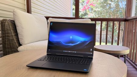
 Gaming LaptopsBest Alienware and Dell deals 2026 — on gaming PCs and gaming laptops
 -
 DealsGet an RTX 5090 gaming laptop for less than $3,000
 -
 DealsSave $300 on Gigabyte's Gaming A16 gaming laptop at Walmart
 -
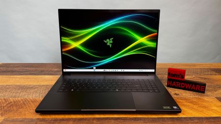 Gaming LaptopsRazer Blade 18 (2026) review: Coming in fast and hot
 -
 DealsGrab an $800 saving on this RTX 5070 Ti gaming laptop from HP with customizable specs and a 20-core CPU
-


-
-
 MacbooksAMD taunts Apple's MacBook Neo for failing to run 75% of top PC games
 -
 Deals$300 slashed from Apple's M4 MacBook Air with 24GB of RAM — get a premium laptop for just $1,099
 -
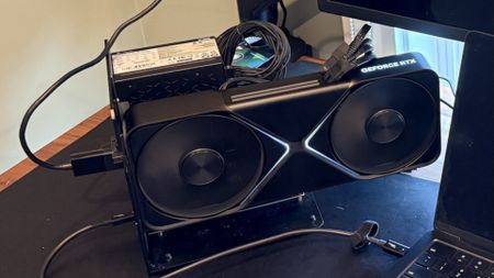 MacbooksM5 Max MacBook Pro paired with RTX 5090 in an eGPU dock
 -
 MacbooksMacBook user explains why he files the sharp metal edges off his Apple laptops
 -
 DealsSave up to $150 on Apple's brand-new M5-powered MacBook Air 13
 -
 MacbooksApple turns 50 — one of the world's biggest tech companies started with hobbyist computers
 -
 MacbooksMacBook Neo mods include copper and liquid cooling — temps drop and boost performance by up to 18%
 -
 MacbooksApple MacBook Air (13-inch, M5) review: Steady as it goes
 -
 MacbooksTim Cook says Apple had its best launch week for first-time Mac customers with the MacBook Neo
-


-
-
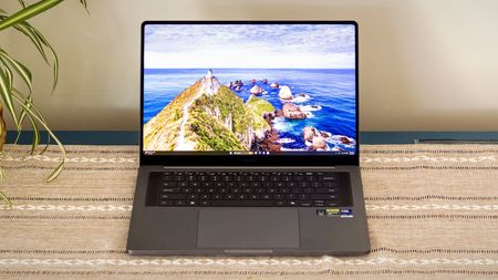
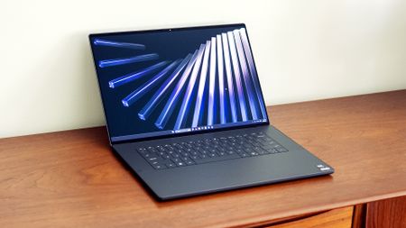 Ultrabooks and UltraportablesDell XPS 16 (2026) Review: A flagship return to form
 -
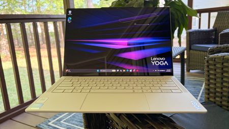 Ultrabooks and UltraportablesLenovo Yoga Slim 7i Aura Edition (2026) Review: Vibrant display, lightweight design, and an endurance champ
 -
 Ultrabooks and UltraportablesAsus Zenbook A16 review: Snapdragon X2 Elite Extreme is a strong chip in a so-so package
 -
 Ultrabooks and UltraportablesChina laptop vendor eats humble pie, apology says ‘production error’ was behind chip mix-up
 -
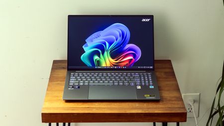 Ultrabooks and UltraportablesAcer Swift 16 AI Review: A Premium contender with a curious twist
 -
 Ultrabooks and UltraportablesApple announces $599 MacBook Neo running A18 Pro chip
 -
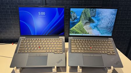 Ultrabooks and UltraportablesLenovo brings a blue ThinkPad T14 to Mobile World Congress
 -
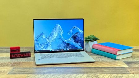
 Ultrabooks and UltraportablesSamsung Galaxy Book6 Ultra review: Premium creator pick
 -
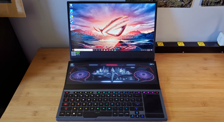
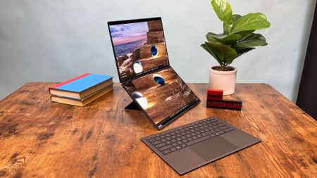 Ultrabooks and UltraportablesAsus Zenbook Duo (2026) review: Premium Panther Lake
-


