AMD Explains Advantages of High Density (Thin) Libraries
At today's Hot Chips Symposium, Mark Papermaster, Senior Vice President and CTO at AMD, talks about the upcoming "High Density (Thin) Libraries"
Get Tom's Hardware's best news and in-depth reviews, straight to your inbox.
You are now subscribed
Your newsletter sign-up was successful
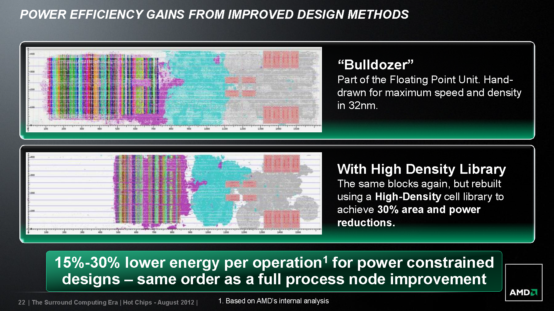
We have seen the improvements that the "Steamroller" will offer in performance per watt with its design improvements. In addition to those improvements, AMD will be using "dense" or "thin" libraries employed by its GPU design teams, but for CPU implementation.
AMD told us that products currently shipping with 32nm use a combination of automated place and route and hand-placed semi-custom design (top plot), which reduces power and area somewhat. To deliver more power efficient computations, AMD has employed a high-density cell library to reduce the area and power by 30 percent (bottom plot). The design yields a more portable and energy efficiency CPU core employing industry standard design methodologies well adapted to a foundry model. These improvements, according to AMD, are yielding a 15 to 30 percent lower energy per operation for power constrained designs, as compared to a full process node improvement.
Look for more details from AMD during Hot Chips Symposium on its Surround Computing and Steamroller.
Article continues belowContact Us for News Tips, Corrections and Feedback
Get Tom's Hardware's best news and in-depth reviews, straight to your inbox.
-
wiyosaya In some respects, this sounds like the programmable gate array concept. It is interesting to see this adapted to non-programmable chip design.Reply
I am somewhat surprised, though, that this implies that such optimization was never before computerized. I would be really surprised if there were no computer optimization of chip layouts before this.
So, is this just AMDs marketing engine at the helm again? -
Ragnar-Kon So more logic in a smaller area. Basically what chip designers have been doing since ICs were first invented. Nothing new...Reply
EDIT: My bad, more logic in a smaller area without a die shrink. So essentially just housecleaning on current libraries. Still clever marketing.It is a die shrink, myyyy baaddddd. Doesn't seem anything like the 3-D transistors used in Intel's 22nm process though. Not that is necessarily a bad thing, I just thought it was similar to that originally. -
ikefu Its also lower power consumption without a die shrink, which means more thermal headroom to up frequencies, add a die shrink on top of this and you suddenly gets LOTS more headroom.Reply
So no, not just good marketing. But I am confused why this didn't happen already.
Doesn't fix their instruction per clock efficiency problem, but it will help increase CPU frequencies to cover for it while they work on that problem. -
Shin-san Okay, what about the performance?!Reply
ikefuIts also lower power consumption without a die shrink, which means more thermal headroom to up frequencies, add a die shrink on top of this and you suddenly gets LOTS more headroom.So no, not just good marketing. But I am confused why this didn't happen already.Doesn't fix their instruction per clock efficiency problem, but it will help increase CPU frequencies to cover for it while they work on that problem.I'm thinking that they are going for raw clocks. -
acadia11 Ragnar-KonSo more logic in a smaller area. Basically what chip designers have been doing since ICs were first invented. Nothing new... move along.But yeah... marketing at its finest (or worst?).EDIT: My bad, more logic in a smaller area without a die shrink. So essentially just housecleaning on current libraries. Still clever marketing.Reply
I thought it was going to be used in asphalt paver?
Ok , I just made that name up there is no chip asphalt paver.
-
blazorthon This could be used in place of a die shrink or at least with a minor die shrink rather than a major die shrink. That's quite something even if it won't be used until Excavator.Reply -
dusk007 I don't get that AMD focus on raw high clocks anyway.Reply
Todays CPUs are constrained by heat and power anyway before the maximum clock is hit.
That is like building an aircraft turbine that can work well at Mach 2 while the entire airframe and efficiency requirements and noise regulations won't let the plane past 950 km/h anyway.
