AMD's HBM Promises Performance Unstifled By Power Constraints
It's been a long time coming; there have been rumblings for a while now that AMD's next generation graphics cards would implement a new memory architecture. There was talk about this being a 3D approach to memory design, but there were no clear details about what that meant. At least, that was the case before today.
AMD claims to have managed to create memory that has higher bandwidth than GDDR5, far better power efficiency than we've seen before, and takes up considerably less physical space while doing it.
Although we still don't know when it will come to market, and the company isn't yet talking specifics, we do know that the first iteration of High Bandwidth Memory (HBM) will be used initially in consumer graphics before being implemented across other divisions. The company sees many uses for HBM in the future and expects to see everything from Compute to APUs take advantage.
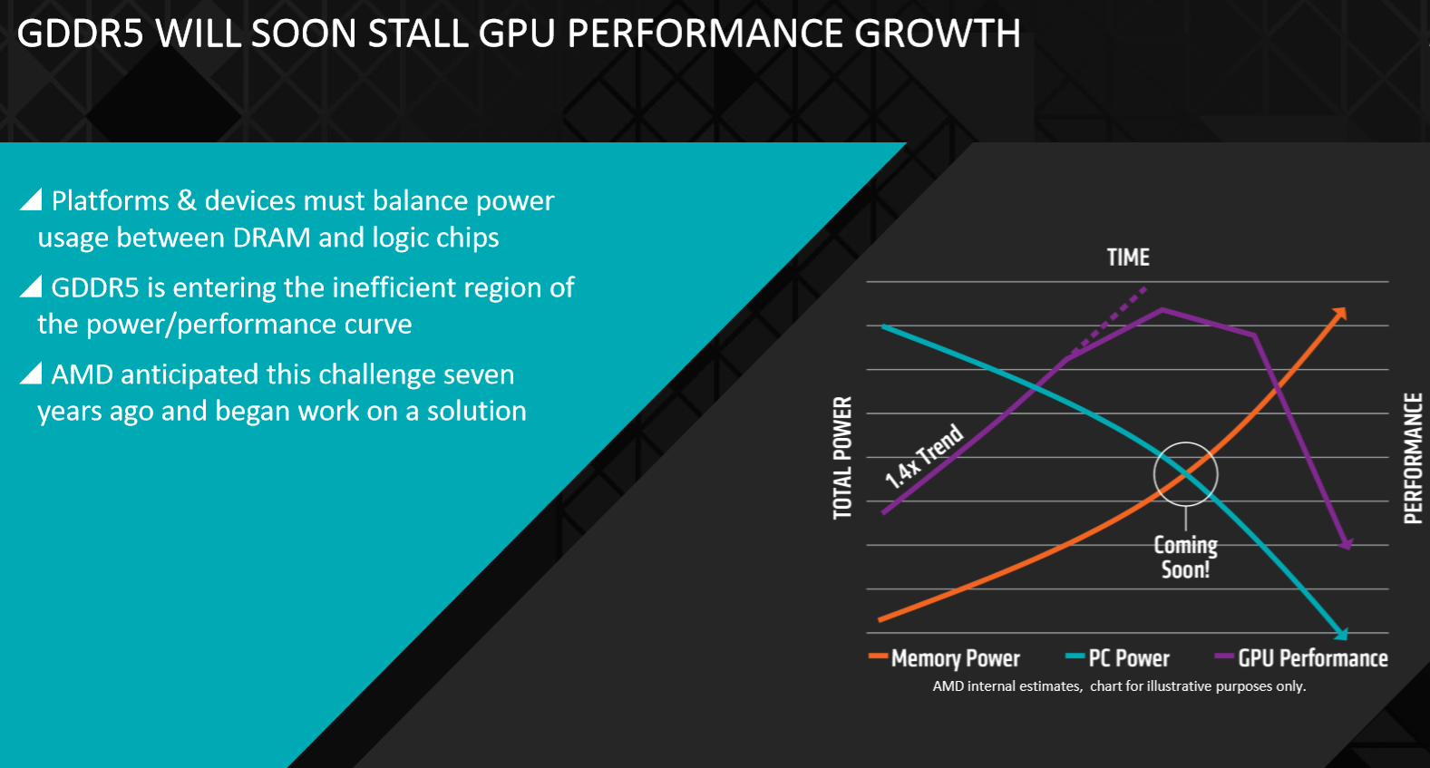
AMD started work on this project over seven years ago. When the engineers first sat down and started thinking about what problems lay ahead, it became apparent to them that bandwidth per watt would quickly become an issue. As bandwidth demands go up, the traditional solution has been to integrate more into the die. DRAM doesn't have that luxury, and yet its bandwidth demands rise as CPUs and GPUs get faster and faster. For GDDR5 to keep up, more power is required, and at a certain point that is no longer feasible.
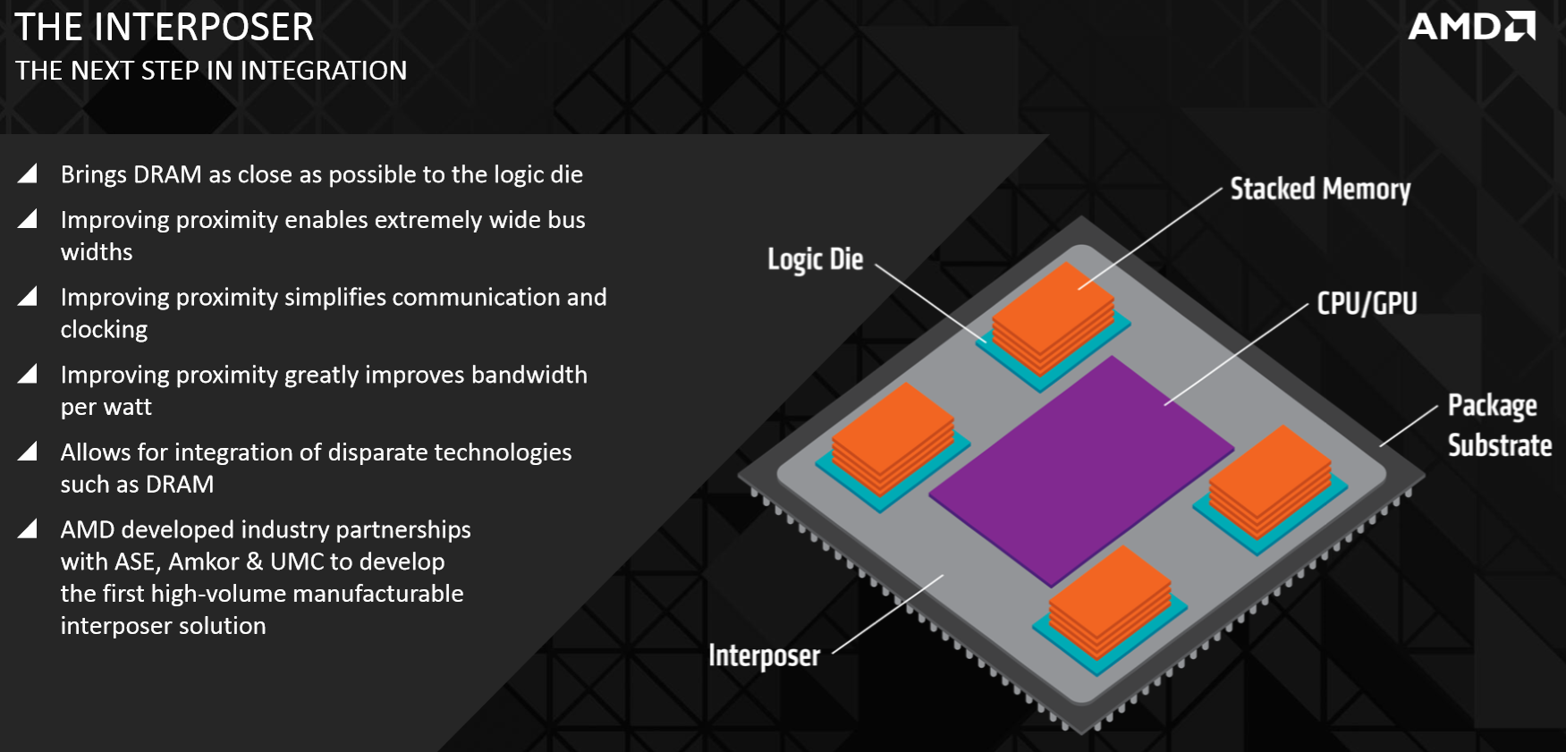
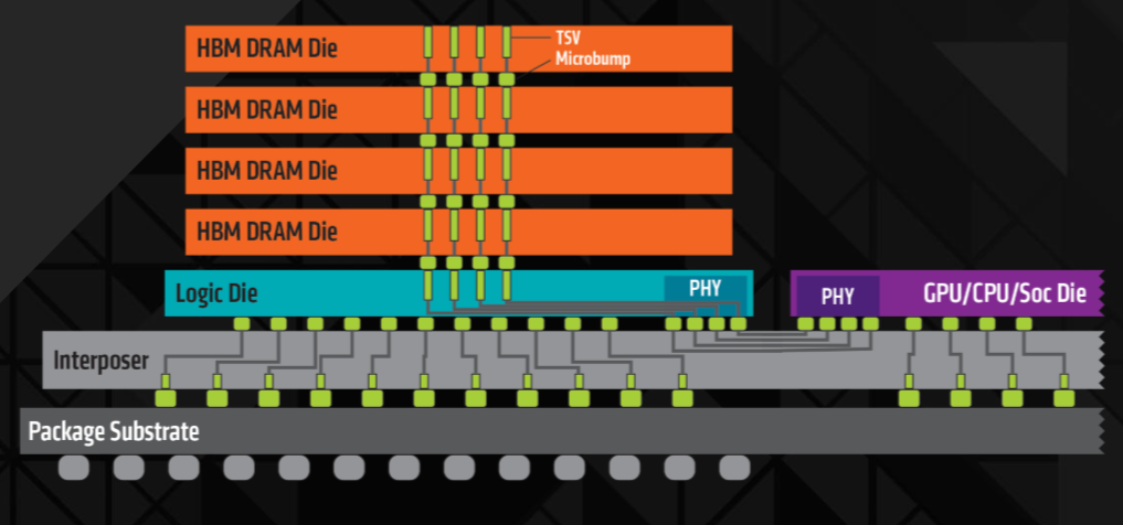
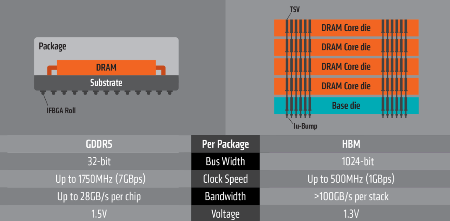
HBM was engineered to help solve that problem. Attacking the issue from all directions, the company came up with what it calls a 3D design, stacking four storage chips on top of a single logic die. This logic die is then attached directly to a silicon based interposer with no active transistors. The GPU, CPU or SoC die is also connected directly to the interposer, which itself is connected to the package substrate.
Because this is a very new approach, a whole new type of interconnects was developed for the stacked memory chips which have been dubbed "through-silicon vias" (TSVs) and "ubumps." These TSVs allow one chip to be connected vertically to the next and are also used to connect the SoC/GPU to the interposer.
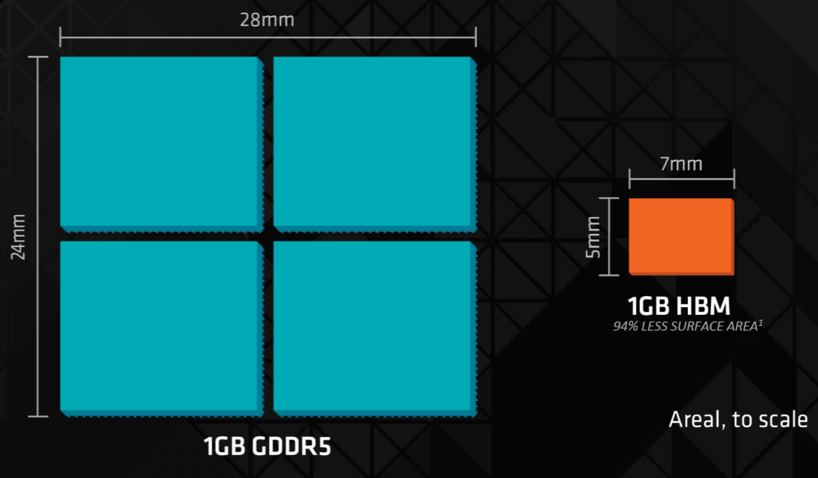
With the memory chips thus stacked, they take up far less space. Where recent graphics cards have had memory chips surrounding most of the GPU die, an HBM configuration would only require four, and they would be positioned in the corners. In this approach there is far less distance for data to travel in order to reach the processor. Not only are there fewer chips, the HBM stacks use up far less surface area than GDDR5 modules. A single 1 GB stack is only 5 x 7 mm, whereas the same volume in GDDR5 would be 28 x 24 mm.
Get Tom's Hardware's best news and in-depth reviews, straight to your inbox.
High Bandwidth Memory resets the clock, so to speak. For years, in order to get more throughput, clock speed increases were necessary. However, the Bus Width that HBM provides negates this need. GDDR5 runs on a 32-bit bus at up to 1750 MHz, which is 7 GB/s. The effective bandwidth can reach 28 GB/s per chip.
HBM, on the other hand, has a Bus Width of 1024-bit and a far lower clock speed of 500 Mhz (1 GBps), and the bandwidth peaks between 100 and 125 GB/s per stack. This is all while improving the bandwidth from 10.66 GB/s per Watt to over 35 GB/s per Watt.
These numbers are for the first generation of the technology, which AMD promised will increase dramatically in the second iteration. Expectations are that the speed will double and the capacity will quadruple by then.
Four times the capacity sounds outrageous, but the first generation is limited to a maximum of 1 GB per stack, and the tech only allows for four stacks to be used. This means the first generation of graphics cards will have frame buffers that max out at 4 GB. This may seem like an issue, but Joe Macri, AMD Product CTO overseeing HBM development, addressed this concern stating his belief that there is no problem that can't be overcome by the company's engineers.
Previously, there were no other options to boost performance other than to increase the frame buffer. There were no engineers working on solving this problem, but now with the way HBM can scale, AMD has put some of its own minds to work on finding more efficient ways to handle memory. It would seem the company is confident that 4 GB of HBM will rival the larger frame buffers that have been popular as of late.
It's only a matter of time before we're able to put AMD's claims about HBM to the test. New GPUs from AMD are expected in the near future, and now that AMD has finally lifted the lid on this well guarded new technology, there must be something coming sooner rather than later. If AMD's claims are to be taken seriously, GPU performance could see a significant leap in the coming year.
Follow us @tomshardware, on Facebook and on Google+.
Kevin Carbotte is a contributing writer for Tom's Hardware who primarily covers VR and AR hardware. He has been writing for us for more than four years.
-
jtd871 Now if the red team can get their overall power use, pricing and performance competitive with the green team at the mainstream level, we all win.Reply -
Memnarchon "Four times the capacity sounds outrageous, but the first generation is limited to a maximum of 1 GB per stack, and the tech only allows for four stacks to be used. This means the first generation of graphics cards will have frame buffers that max out at 4 GB."Reply
This is a confirmation of what we knew.
So I guess 390 and 390X would be 4GB cards? -
serendipiti What about latencies ? at a 500Mhz clock, seems impossible to improve latencies...Reply -
plasmastorm Im fully expecting the issue that Nvidia had a while back with the GPU solder joints failing over time to hit HBM.Reply
Hope it doesn't but something is telling me to be wary -
junkeymonkey ''AMD started work on this project over 7 years ago. When the engineers first sat down and started thinking about what problems lay ahead, it became apparent to them that bandwidth per watt would quickly become an issue. As bandwidth demands go up, the traditional solution has been to integrate more into the die. DRAM doesn't have that luxury, and yet its bandwidth demands rise as CPUs and GPUs get faster and faster. For GDDR5 to keep up, more power is required, and at a certain point that is no longer feasible. ''Reply
so is it that AMD's next generation gpu chips going to be so powerful that they need to get this HBM mainstream ??
seeing that the r9 300 is going to be for the most part refresh/ tweaked r9 200 chips that will be use to work the bugs out of this new memory array then ''next year'' have a new die for a r9 400 card line up that twice as powerful to the point todays ddr5 layout will not be able to keep up with them ??
that statement '' '' above is interesting to what may be coming down the road and the stage is being set for that ..??
-
Larry Litmanen AMD always promises and usually underdelivers, until i will see a card on the market that costs the same as an Nvidia, eats just as much power and gives meaningfully higher FPS i do not want to hear from AMD.Reply
I don't care about technology, is it staked or whatever, is it better? -
CaedenV ReplyWhat about latencies ? at a 500Mhz clock, seems impossible to improve latencies...
Latency in graphics is all about completing the task and exporting a frame every 1/60th (or 1/144th for OC'd panels) of a second. As long as it can render a frame at 60 or 140 Hz then it is fine. At 500,000,000Hz and super high bandwidth I really don't think that latency is going to be a noticeable issue. On the GPU side they may need to increase their buffer size a little bit to compensate for the lower clock rate and the insane increase in input, but that goes up with each generation anyways. -
InvalidError Reply
HBM is coming around because GDDR is no longer able to push the GB/W expected in modern applications. With all GPU designers likely to switch over to HBM, it seems unlikely anyone will bother pushing for GDDR6/7. The problem with off-package memory is that you end up wasting tons of power on bus termination, de-skew, signal equalization, etc. and this gets worse as speeds go up. With HBM, the bus lines are too short for most of these to matter. At least for now.15888248 said:Aside from HBM, is there any sign of say a GDDR6 on the horizon?
The next step after HBM would be direct TSV connection between the RAM and GPU/CPU/whatever - skip the interposer and intermediate glue logic altogether.

