Sandisk and SK hynix join forces to standardize High Bandwidth Flash memory, a NAND-based alternative to HBM for AI GPUs — Move could enable 8-16x higher capacity compared to DRAM
Tackling AI memory from a different angle.

Get Tom's Hardware's best news and in-depth reviews, straight to your inbox.
You are now subscribed
Your newsletter sign-up was successful
Sandisk and SK hynix have just signed a memorandum of understanding to collaborate on what could become a pivotal advancement in AI memory infrastructure. Announced in a press release, this agreement aims to standardize “High Bandwidth Flash” (HBF), a NAND flash-based memory technology built into HBM-like packages. This marks the first serious industry push to fuse flash and DRAM-like bandwidth into a single stack, potentially transforming how AI models access and process data at scale.
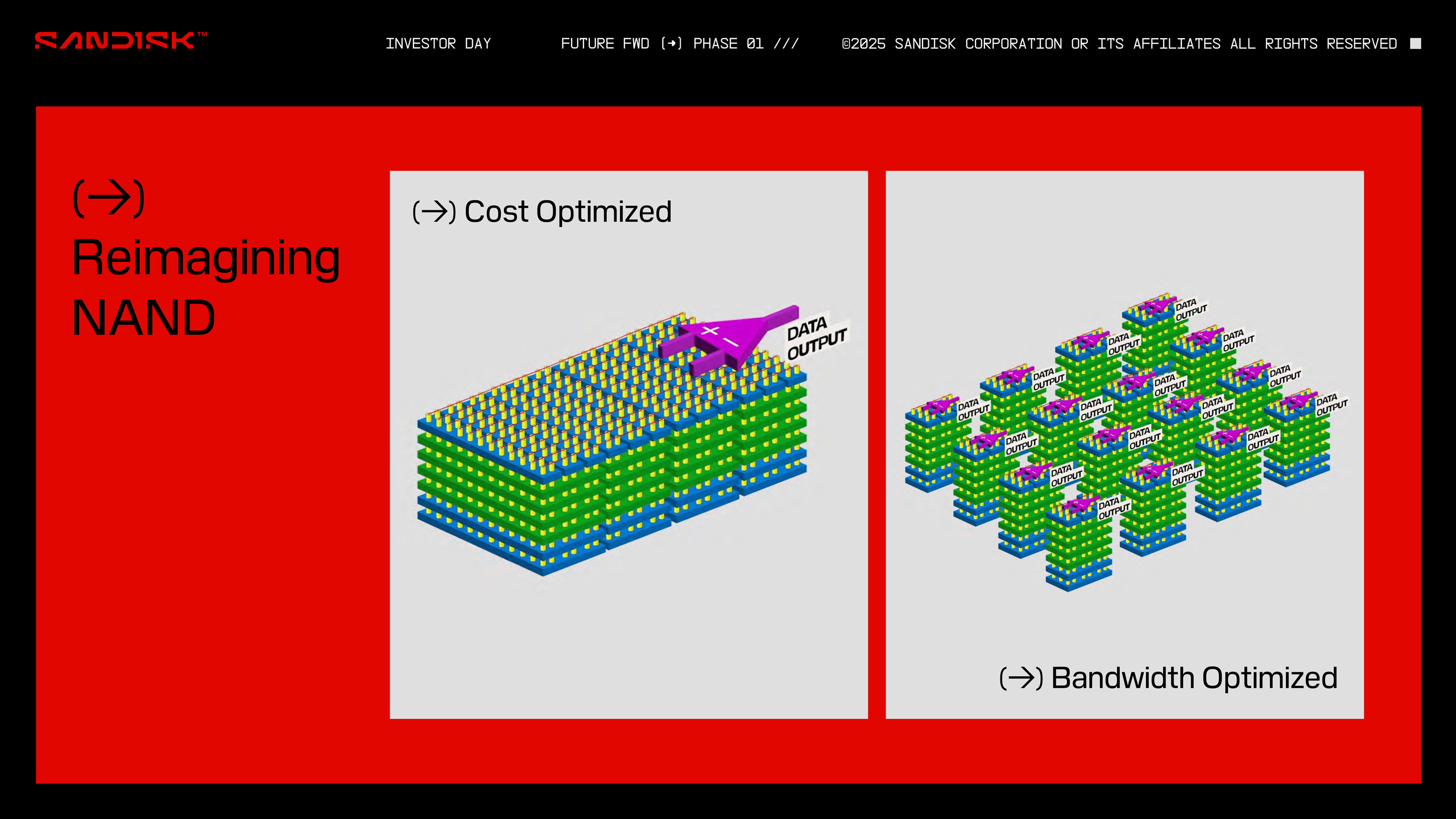
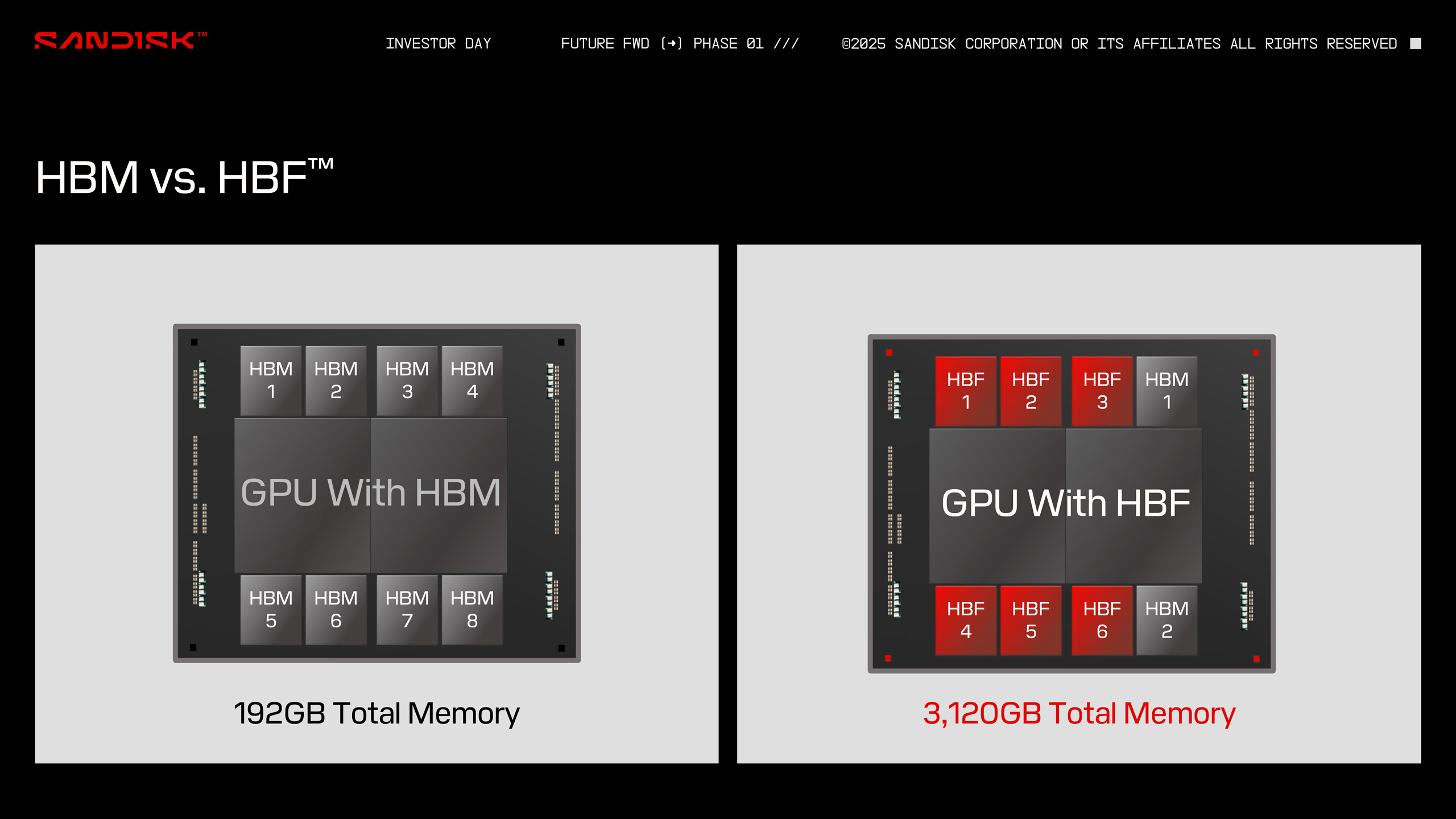
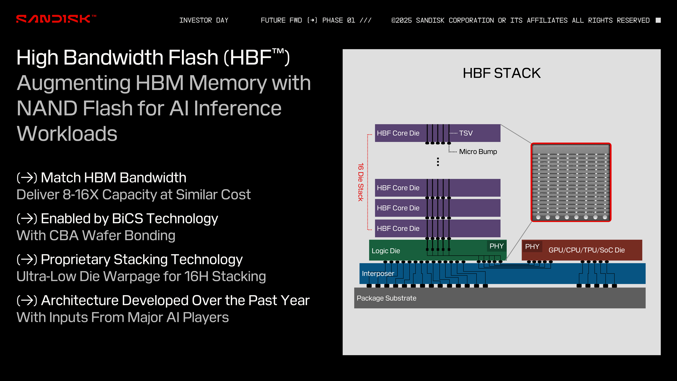
Unlike traditional HBM, which relies exclusively on DRAM, HBF substitutes parts of the memory stack with NAND flash—trading raw latency for significantly higher capacity and non-volatility. The approach allows HBF to deliver up to 8–16x the capacity of DRAM-based HBM, at comparable costs, while still targeting similar bandwidth levels. Unlike DRAM, which requires constant power to retain data, NAND is non-volatile, enabling persistent storage with reduced energy demands.
That distinction is critical as AI inference scales out to more energy-constrained deployments. Hyperscalers (companies with massive cloud infrastructure for rent) are now pushing inference to the edge, and cooling budgets in AI data centers are already hitting practical limits.

A couple of years ago, a widely-discussed research paper titled “LLM in a Flash” proposed an architecture where large language models could be efficiently run by using SSDs as an additional memory tier, offloading some of the memory pressure from DRAM. Therefore, by marrying NAND flash’s high capacity with interface designs inspired by HBM’s bandwidth capabilities, Sandisk and SK hynix are effectively proposing a new memory class — one that could support large model inference without incurring the thermal and cost overheads of traditional HBM stacks.
The move is also aligned with broader industry shifts. Samsung, for instance, recently unveiled its own flash-backed AI storage tier dubbed “PBSSD” and is actively working on next-gen HBM4 DRAM expected to include logic die integration and potentially hybrid stacks. Meanwhile, Nvidia's roadmap through its Rubin and Vera GPUs continues to rely heavily on HBM, and integrating flash may offer a path to scale memory without linearly scaling cost and power. You can see our deep-dive into HBM roadmaps for Samsung, Micron, SK hynix to learn more.
Sandisk’s HBF prototype, shown at the Flash Memory Summit 2025, was developed using its proprietary BiCS NAND and CBA wafer bonding technologies. The company received the “Most Innovative Technology” award at the event, and announced the formation of a Technical Advisory Board to guide HBF’s development and ecosystem strategy. The board includes figures from both inside and outside Sandisk, underscoring the company's intent to establish HBF as a cross-industry standard, not just a proprietary product.

Sample HBF modules are expected in the second half of 2026, with the first AI inference hardware integrating the tech anticipated in early 2027. While no specific devices or partners have been named, industry watchers speculate that SK hynix's close relationship with Nvidia and other AI chipmakers could accelerate adoption once standards are in place. Previously, Raja Koduri, Intel's former graphics chief and now running his own startup, also joined hands with Sandisk to advise on HBF for AI GPUs.
Get Tom's Hardware's best news and in-depth reviews, straight to your inbox.
If successful, this collaboration could pave the way for heterogeneous memory stacks where DRAM, flash, and potentially even new persistent memory types coexist within AI accelerators. In doing so, it could also give hyperscalers a much-needed alternative to escalating HBM costs while enabling next-gen models that are increasingly bumping against memory ceilings. After all, SK hynix is already the world's top-selling memory maker, so they stand to gain from any potential substitutes developed in-house.
This is also not uncharted territory for Sandisk as the firm has a long-standing history of collabs and most recently partnered with Kioxia, the inventor of flash, to develop BiCS9 using CMOS processes. Despite the fact that HBF is utilizing CBA-based BiCS NAND, Sandisk did not confirm whether it's the same generation it has worked with Kioxia on. We will update the article if new information surfaces.
Follow Tom's Hardware on Google News to get our up-to-date news, analysis, and reviews in your feeds. Make sure to click the Follow button.

Hassam Nasir is a die-hard hardware enthusiast with years of experience as a tech editor and writer, focusing on detailed CPU comparisons and general hardware news. When he’s not working, you’ll find him bending tubes for his ever-evolving custom water-loop gaming rig or benchmarking the latest CPUs and GPUs just for fun.
-
we_are_theBorg Oh great.... I'm sure all the big AI hardware vendors are salivating at the idea of inserting a NAND write endurance based death clock in to all of their new products... good luck picking these up on the secondary market,Reply
Fantastic.
Ironically this is where something like Optane would be perfect. Higher density than DRAM, lower latency than NAND, massive write endurance. Cost premium insensitive. Hello Intel, get your butt off the floor and figure out the licensing! -
deesider Reply
I think it's all too easy to view Optane through rose-coloured glasses, and ignore the issues that prevented it from becoming successful - namely high power usage, and lack of scalability rather than miss-management.we_are_theBorg said:Oh great.... I'm sure all the big AI hardware vendors are salivating at the idea of inserting a NAND write endurance based death clock in to all of their new products... good luck picking these up on the secondary market,
Fantastic.
Ironically this is where something like Optane would be perfect. Higher density than DRAM, lower latency than NAND, massive write endurance. Cost premium insensitive. Hello Intel, get your butt off the floor and figure out the licensing!
- The high power usage prevented it from being used in most consumer devices, which are largely power-sensitive laptops and phones.
- The lack of scalability seems to be due to either fabrication or design limitations that prevent it from being layered like conventional NAND. Being able to fabricate dozens of layers of NAND at once was a major breakthrough that finally provided relatively cheap SSDs. It seems that wasn't possible with Optane, either due to its design (which may also be why it operates so much faster) or it could be impractical to have that many layers of a temperature sensitive material crammed together.
A good comparison would be plasma TVs. They were still the benchmark for picture quality for at least 5 years after production was ceased, but ultimately, despite the advantages, were a dead-end technology - more expensive to manufacture than LCDs, and the cells couldn't be made small enough for 4k resolution - which apparently was what the market demanded. -
we_are_theBorg Reply
I appreciate your point on Optane power density. Still, in this case I feel like this application is one where that and the density issue (which I did address) are not deal breakers in this application, while the latency benefits and write endurance are very relevant.deesider said:I think it's all too easy to view Optane through rose-coloured glasses, and ignore the issues that prevented it from becoming successful - namely high power usage, and lack of scalability rather than miss-management.
- The high power usage prevented it from being used in most consumer devices, which are largely power-sensitive laptops and phones.
- The lack of scalability seems to be due to either fabrication or design limitations that prevent it from being layered like conventional NAND. Being able to fabricate dozens of layers of NAND at once was a major breakthrough that finally provided relatively cheap SSDs. It seems that wasn't possible with Optane, either due to its design (which may also be why it operates so much faster) or it could be impractical to have that many layers of a temperature sensitive material crammed together.
A good comparison would be plasma TVs. They were still the benchmark for picture quality for at least 5 years after production was ceased, but ultimately, despite the advantages, were a dead-end technology - more expensive to manufacture than LCDs, and the cells couldn't be made small enough for 4k resolution - which apparently was what the market demanded.
In the end it's moot, of course. That ship has sailed. Maybe UltraRAM will save us.
My fundamental point is to be wary of any technology that adds an intrinsic death clock to devices that should be in the infrastructure category instead of the consumables category. "My GPU has run out of write endurance" is not something consumers or IT budget managers should be cool with.