Kioxia and SanDisk start shipping BiCS9 3D NAND samples — hybrid design combining 112-layer BiCS5 with modern CBA and Toggle 6.0 interface for higher performance and cost efficiency
A transitional step for manufacturing and performance tuning ahead of BiCS10’s more complex, high-density architecture.
Get Tom's Hardware's best news and in-depth reviews, straight to your inbox.
You are now subscribed
Your newsletter sign-up was successful
Kioxia and SanDisk have begun sample shipments of their ninth-generation BiCS FLASH, a NAND flash technology that blends legacy architectures with modern enhancements to create a bridge between the current BiCS8 generation and the forthcoming BiCS10. While BiCS10 is expected to deliver higher capacities through a cutting-edge 332-layer design, BiCS9 takes a more cost-optimized approach, targeting enterprise SSDs built for AI workloads and mid-tier storage solutions where efficiency and performance balance are key.
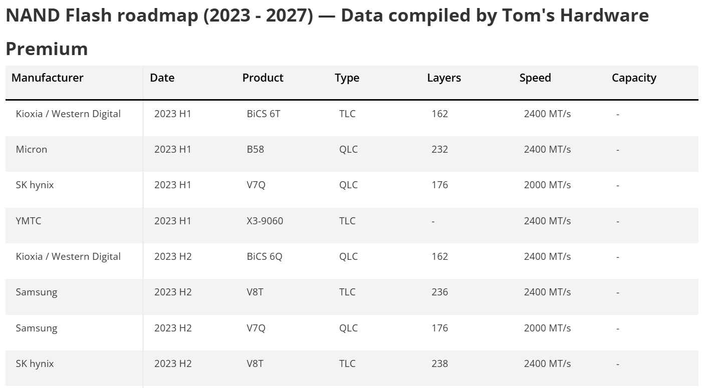
Want more? We've got an exclusive roadmap to the future of 3D NAND flash — only for subscribers of Tom's Hardware Premium.
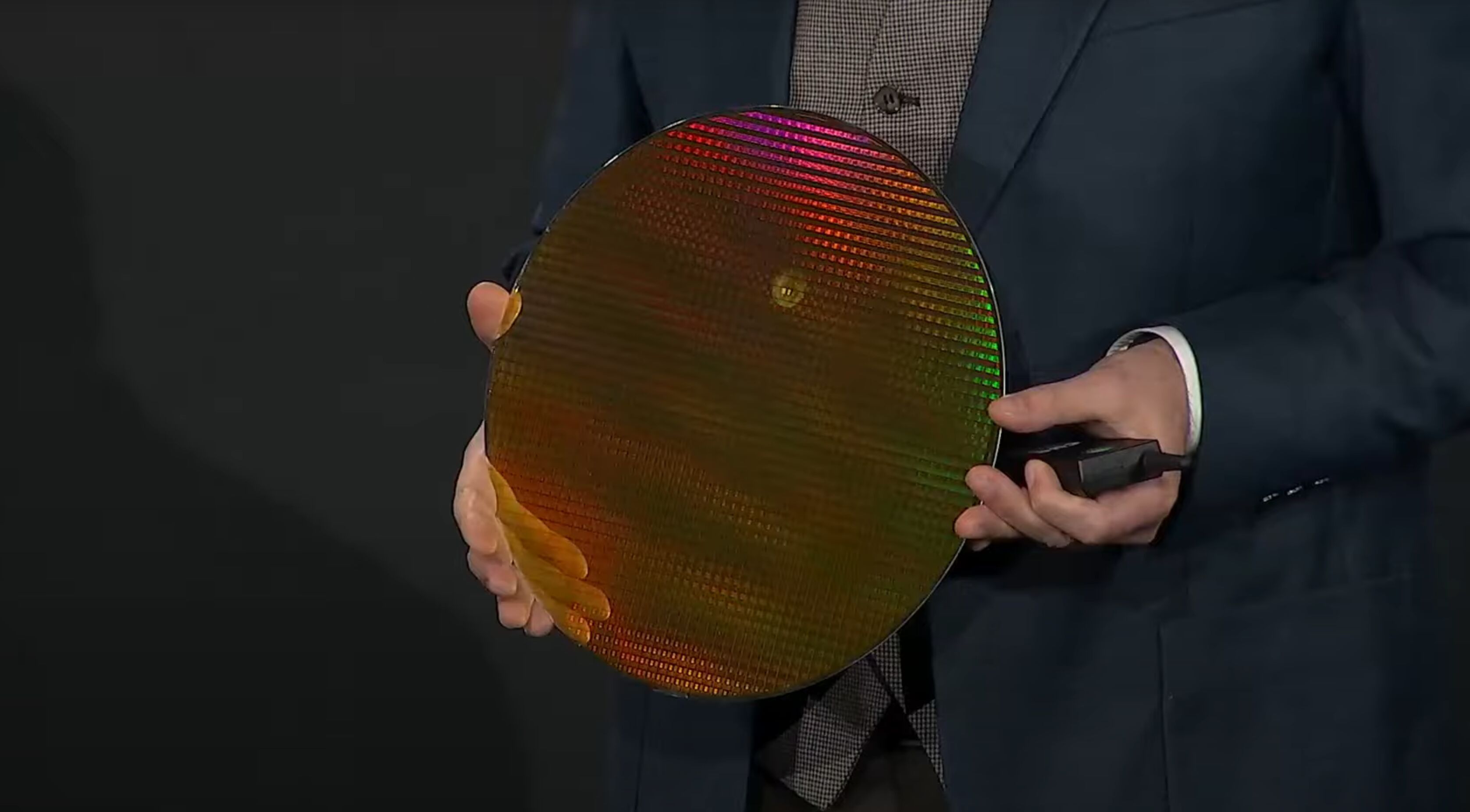
What sets BiCS9 apart is its hybrid construction, achieved through CMOS directly Bonded to Array (CBA) technology. In this process, the logic and memory cell wafers are fabricated separately under optimized conditions before being bonded into a single, high-performance package. This innovation allows Kioxia to mix and match mature cell structures—such as a 112-layer BiCS5 or a 218-layer BiCS8—with a modern I/O interface. The result is a chip capable of delivering Toggle DDR 6.0 speeds of up to 3.6 Gb/s, with peak speeds reaching 4.8 Gb/s under controlled testing conditions.
Despite employing fewer layers than BiCS8 or the next-gen BiCS10, BiCS9 still brings meaningful upgrades. Write performance is up by 61%, read speeds improve by 12%, and power efficiency rises by 36% during writes and 27% during reads compared to previous 512 GB TLC designs. An 8% increase in bit density further underscores the careful engineering that allows BiCS9 to deliver strong performance without inflating costs.
Article continues below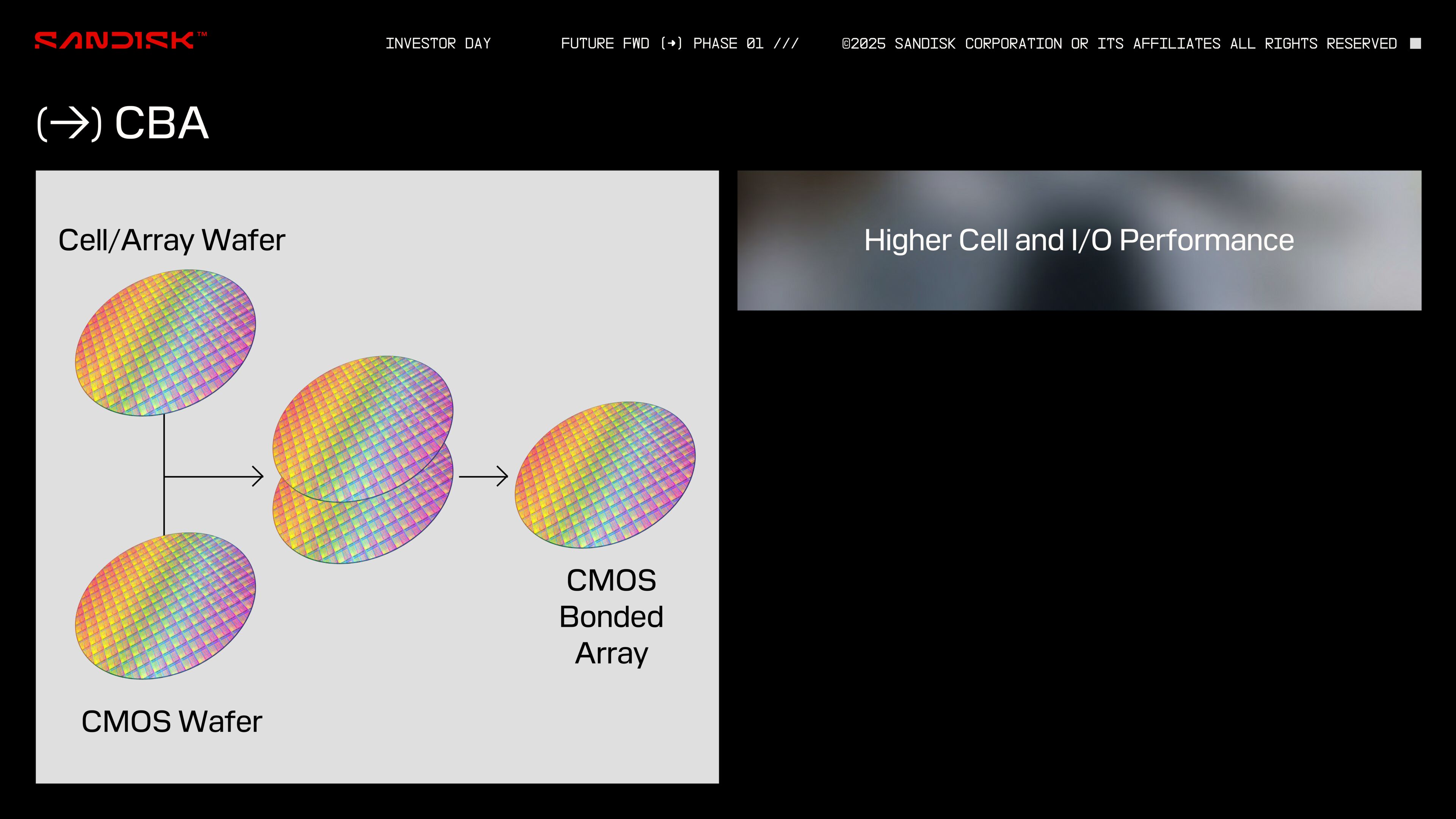
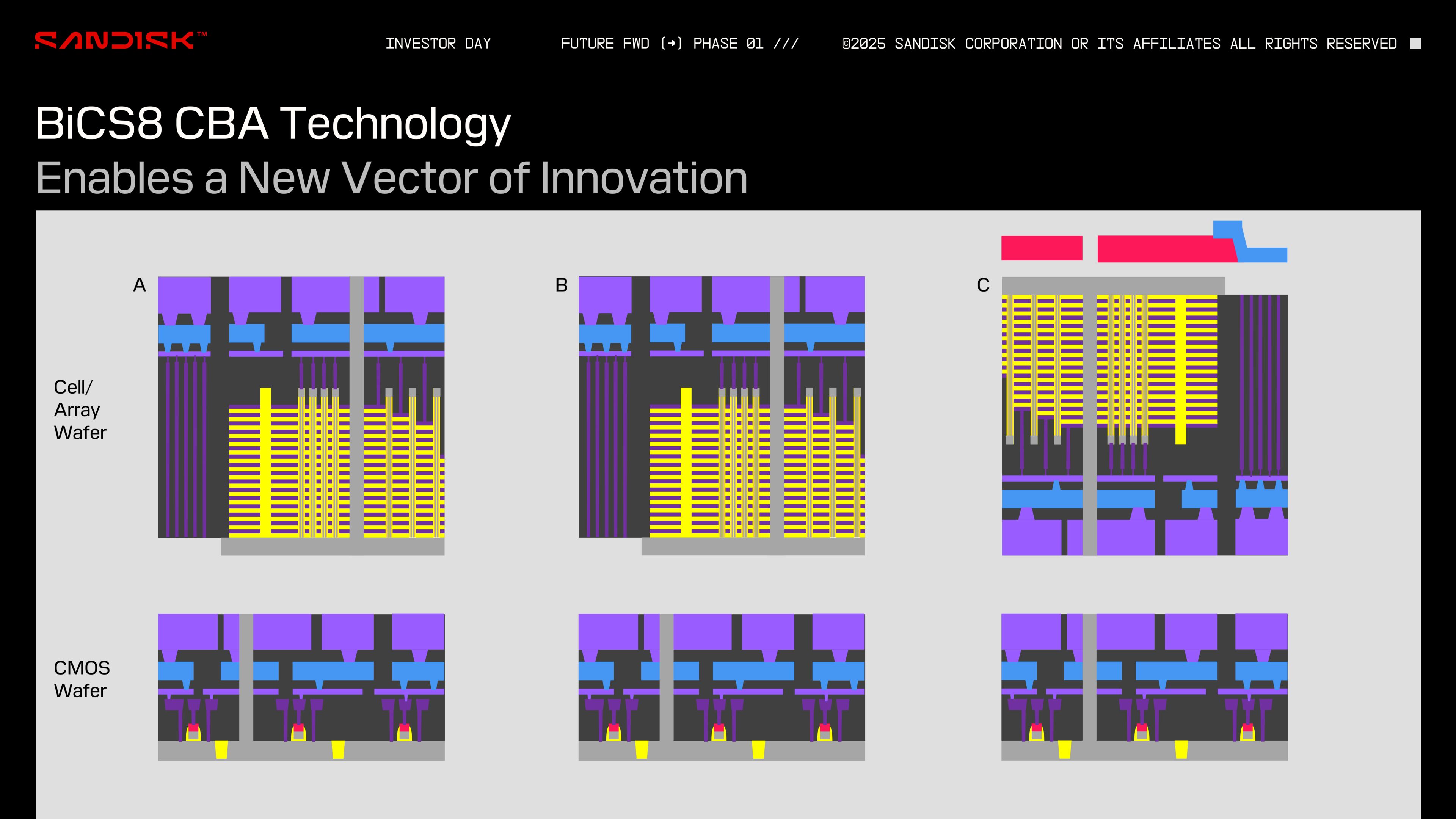
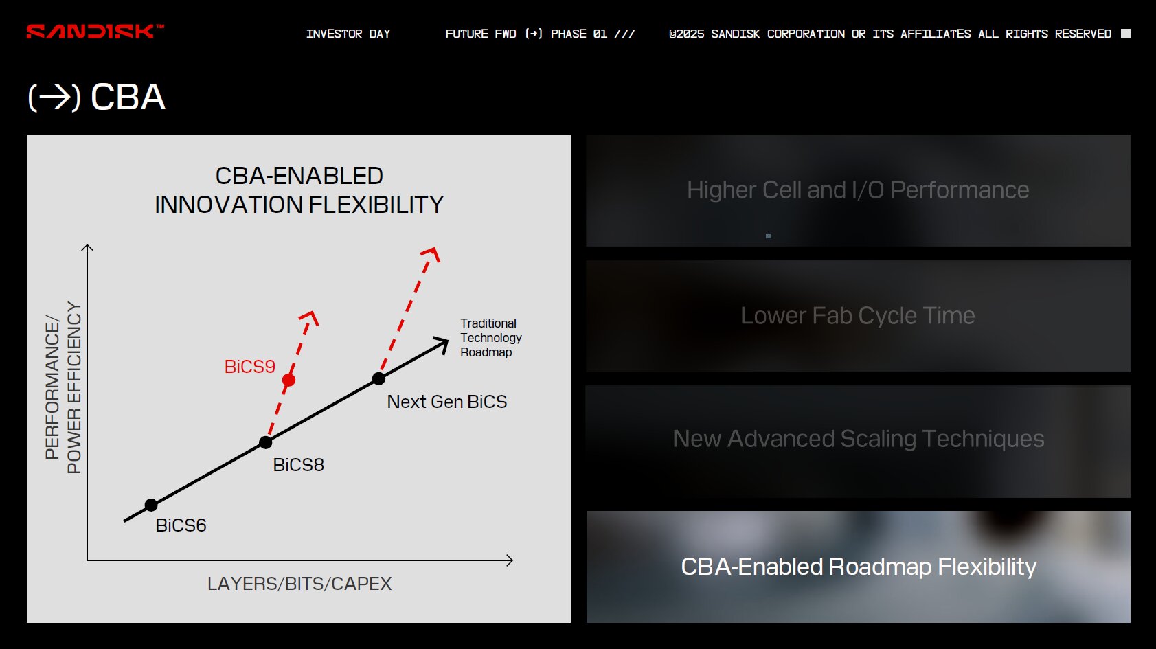
Kioxia’s roadmap positions BiCS9 as a transitional step, enabling the company to refine manufacturing techniques and performance tuning ahead of BiCS10’s more complex, high-density architecture. This strategy is particularly relevant as AI-driven data workloads demand faster, power-conscious storage solutions capable of feeding GPUs with minimal latency, especially with the extreme ambition associated with the AI boom.
Kioxia’s approach with BiCS9 contrasts with rivals like Samsung and Micron, who are betting on aggressively scaling layer counts to achieve capacity gains. While competitors push beyond 300 layers, Kioxia is focusing on hybrid architectures that offer faster time-to-market and better cost efficiency. Working with a consumer-facing industry veteran like SanDisk ensures Kioxia, who invented NAND flash, stays highly competitive through mixed R&D efforts.
Therefore, the company's long-standing partnership with SanDisk has been instrumental in shaping the BiCS series, combining Japanese manufacturing expertise with SanDisk’s deep storage market presence. Since their joint venture began in 2006, the two companies have co-developed multiple generations of 3D NAND technology, pushing the limits of scaling and performance. BiCS9 serves as their new marquee offering, alongside Kioxia's own efforts to set new industry standards.
Follow Tom's Hardware on Google News to get our up-to-date news, analysis, and reviews in your feeds. Make sure to click the Follow button.
Get Tom's Hardware's best news and in-depth reviews, straight to your inbox.

Hassam Nasir is a die-hard hardware enthusiast with years of experience as a tech editor and writer, focusing on detailed CPU comparisons and general hardware news. When he’s not working, you’ll find him bending tubes for his ever-evolving custom water-loop gaming rig or benchmarking the latest CPUs and GPUs just for fun.
-
usertests Confusing but interesting.Reply
This innovation allows Kioxia to mix and match mature cell structures—such as a 112-layer BiCS5 or a 218-layer BiCS8—with a modern I/O interface.
So higher speed NAND with denser NAND?
The result is a chip capable of delivering Toggle DDR 6.0 speeds of up to 3.6 Gb/s, with peak speeds reaching 4.8 Gb/s under controlled testing conditions.
I take it that is unrelated to DDR6 DRAM? -
JRStern Reply
I dunno either, I could guess but hey.usertests said:Confusing but interesting.
...
I take it that is unrelated to DDR6 DRAM?
Maybe it has to do with new memory architecture I've seen mentioned, no more disk interface, no more PCI interface, it can write big blocks faster to DRAM, this makes the AI guys happy, possibly an alternative to HBM. -
thestryker Reply
Correct it's an interface standard and "Toggle" is the important word here (the headline should probably be changed). I'd not seen the terminology before either and went searching and this was the first thing I saw which just explained it:usertests said:I take it that is unrelated to DDR6 DRAM?
https://phisonblog.com/nand-flash-101-flash-device-interfaces-2/