Nvidia asked SK hynix to accelerate HBM4 chip delivery by six months, says report
So, HBM4 may arrive earlier than indicated on previous roadmaps.

Nvidia has asked SK hynix to move up its delivery timeline for next-generation HBM4 memory chips by six months, according to SK Group Chairman Chey Tae-won, reports Reuters.
Initially, SK hynix planned to ship its HBM4 chips to customers in the latter half of 2025. Following Nvidia CEO Jensen Huang's request, the timeline was shortened, though the exact new schedule was not specified. Nvidia is currently working on its next-generation GPUs for AI and HPC that will use HBM4 memory (presumably codenamed Rubin). So the company must lay its hands on next-generation high-bandwidth memory sooner rather than later.
SK hynix continues to solidify its lead in the HBM market, propelled by increased demand from the AI industry. The company supplied Nvidia with 8-Hi and 12-Hi HBM3E for the company's current-generation products and, looking ahead, SK hynix plans to launch 12-layer HBM4 next year and aims to roll out a 16-layer version by 2026, aligning with anticipated industry needs.
Initially, SK Hynix was leaning towards using 1b DRAM technology for its HBM4 layers, but Samsung's choice of the more advanced 1c production technology has reportedly prompted SK hynix to reevaluate its approach.
The upcoming HBM4 standard will introduce memory layers of 24Gb and 32Gb, along with stacking options of 4-high, 8-high, 12-high, and 16-high TSV stacks. The exact configurations of initial HBM4 modules are still uncertain, Samsung and SK hynix plan to begin mass production of 12-high HBM4 stacks in the latter half of 2025. Speed bins of these modules will vary, depending on numerous factors, but JEDEC's preliminary standards set speeds of up to 6.4 GT/s.
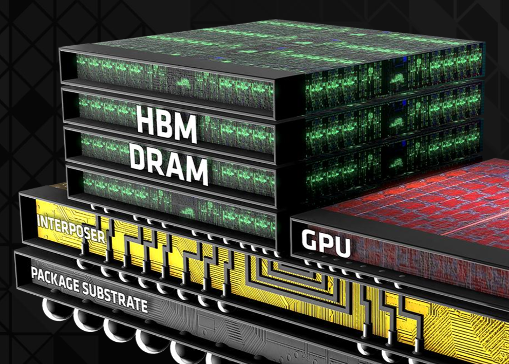
To manufacture base dies for its HBM4 modules, SK hynix is partnering with TSMC. At the European Technology Symposium 2024, TSMC disclosed that it would produce these base dies using its 12FFC+ (12nm-class) and N5 (5nm-class) process technologies. The N5 process will enable higher logic density and finer interconnect pitches, which will allow memory to be directly integrated into CPUs and GPUs. Alternatively, the 12FFC+ process will provide a more cost-effective solution by using silicon interposers to connect memory with host processors, striking a balance between performance and affordability.
Get Tom's Hardware's best news and in-depth reviews, straight to your inbox.

Anton Shilov is a contributing writer at Tom’s Hardware. Over the past couple of decades, he has covered everything from CPUs and GPUs to supercomputers and from modern process technologies and latest fab tools to high-tech industry trends.