Chinese Biren's New GPUs Have 77 Billion Transistors, 2 PFLOPS of AI Performance
Chinese GPU developer introduces a 77 billion transistors chip.
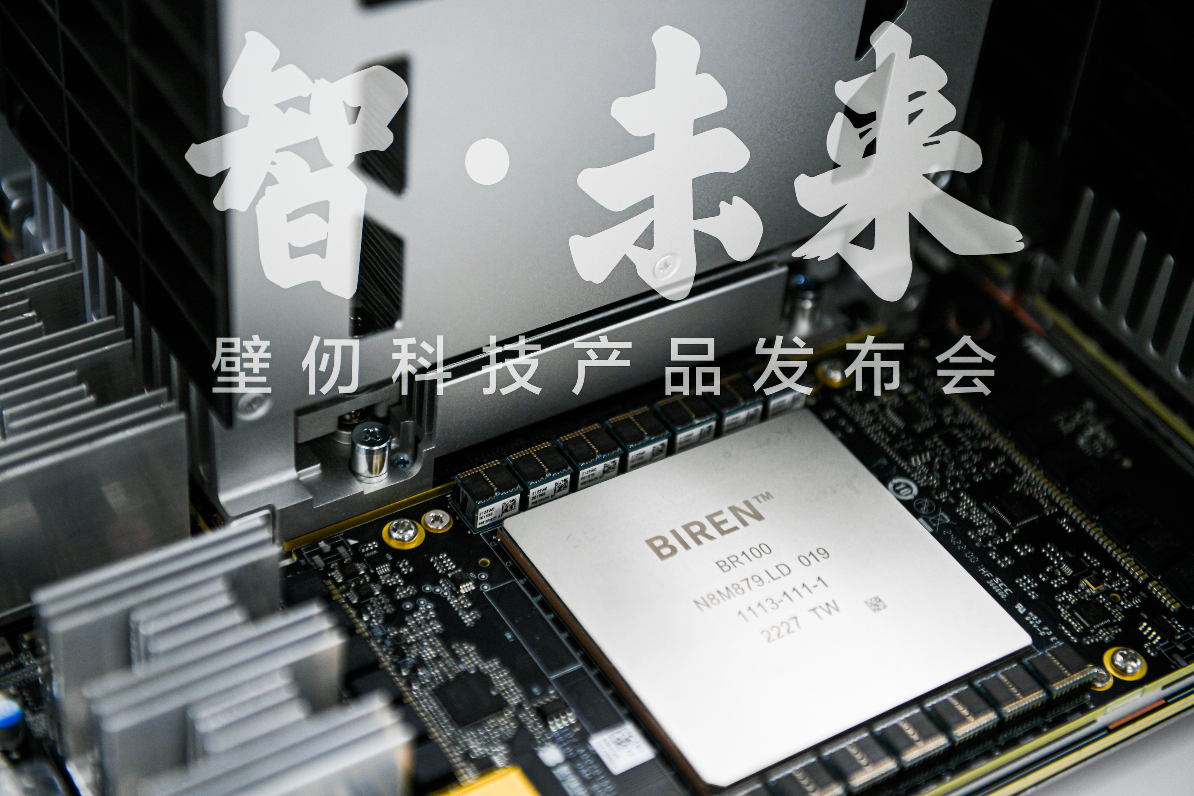
Biren Technology has formally introduced its first GPUs designed primarily for artificial intelligence (AI) and high-performance computing (HPC). According to the company, the top-of-the-range BR100 GPU can challenge Nvidia's A100 and even H100 chips in certain workloads, yet its complexity is comparable with that of Nvidia's H100 compute GPU.
Biren's initial family of compute GPUs includes two chips. The BR100 promises up to 256 FP32 TFLOPS or 2 INT8 PetaFLOPS performance, whereas the BR104 is rated for up to 128 FP32 TFLOPS or 1 INT8 PetaFLOPS performance.
The top-of-the-range BR100 comes with 64GB of HBM2E memory with a 4096-bit interface (1.64 TB/s), while the midrange BR104 with 32GB of HBM2E memory with a 2048-bit interface (819 GB/s).
| Row 0 - Cell 0 | Biren BR104 | Biren BR100 | Nvidia A100 | Nvidia H100 |
| Form-Factor | FHFL Card | OAM Module | SXM4 | SXM5 |
| Transistor Count | ? | 77 billion | 54.2 billion | 80 billion |
| Node | N7 | N7 | N7 | 4N |
| Power | 300W | 550W | 400W | 700W |
| FP32 TFLOPS | 128 | 256 | 19.5 | 60 |
| TF32+ TFLOPS | 256 | 512 | ? | ? |
| TF32 TFLOPS | ? | ? | 156/312* | 500/1000* |
| FP16 TFLOPS | ? | ? | 78 | 120 |
| FP16 TFLOPS Tensor | ? | ? | 312/624* | 1000/2000* |
| BF16 TFLOPS | 512 | 1024 | 39 | 120 |
| BF16 TFLOPS Tensor | ? | ? | 312/624* | 1000/2000* |
| INT8 | 1024 | 2048 | ? | ? |
| INT8 TFLOPS Tensor | ? | ? | 624/1248* | 2000/4000* |
* With sparsity
Both chips support the INT8, FP16, BF16, FP32, and TF32+ data formats, so we're not talking about supercomputing formats (e.g., FP64) even though Biren says that its TF32+ format provides higher data precision than traditional TF32. Meanwhile, the BR100 and BR104 offer rather formidable peak performance numbers. In fact, if the company had incorporated GPU-specific functionality (texture units, render back ends, etc.) into its compute GPUs and had designed proper drivers, these chips would have been rather incredible GPUs (at least BR104, which is presumably a single-chip configuration).
In addition to the compute capabilities, Biren's GPUs can also support H.264 video encoding and decoding.
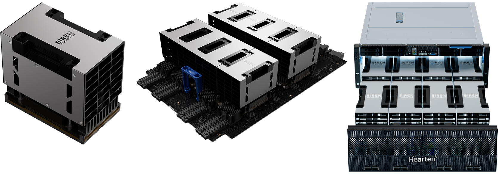
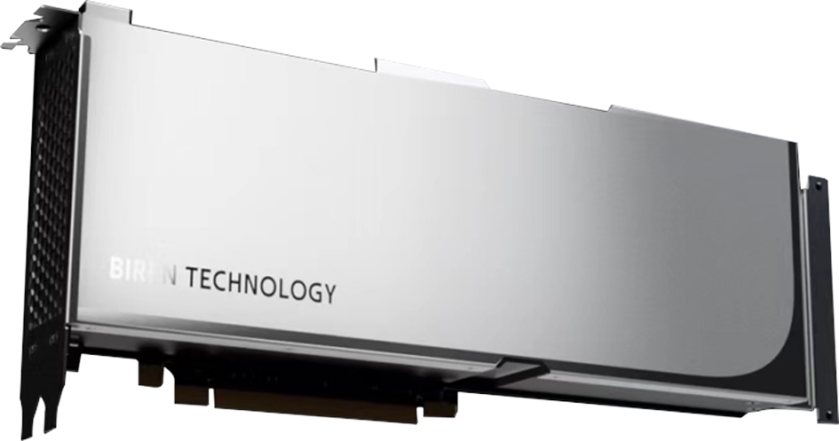
Biren's BR100 will be available in an OAM form-factor and consume up to 550W of power. The chip supports the company's proprietary 8-way BLink technology that allows the installation of up to eight BR100 GPUs per system. In contrast, the 300W BR104 will ship in a FHFL dual-wide PCIe card form-factor and support up to 3-way multi-GPU configuration. Both chips use a PCIe 5.0 x16 interface with the CXL protocol for accelerators on top, reports EETrend (via VideoCardz).
Biren says that both of its chips are made using TSMC's 7nm-class fabrication process (without elaborating whether it uses N7, N7+, or N7P). The larger BR100 packs 77 billion transistors, outweighing the 54.2 billion with the Nvidia A100 that's also made using one of TSMC's N7 nodes. The company also says that to overcome limitations imposed by TSMC's reticle size, it had to use chiplet design and the foundry's CoWoS 2.5D technology, which is completely logical as Nvidia's A100 was approaching the size of a reticle and the BR100 is supposed to be even larger given its higher transistor count.
Get Tom's Hardware's best news and in-depth reviews, straight to your inbox.
Given the specs, we can speculate that BR100 basically uses two BR104s, though the developer has not formally confirmed that.
To commercialize its BR100 OAM accelerator, Biren worked with Inspur on an 8-way AI server that will be sampling starting Q4 2022. Baidu and China Mobile will be among the first customers to use Biren's compute GPUs.

Anton Shilov is a contributing writer at Tom’s Hardware. Over the past couple of decades, he has covered everything from CPUs and GPUs to supercomputers and from modern process technologies and latest fab tools to high-tech industry trends.
-
bit_user Well, here we are. I think Nvidia doesn't really need to worry quite yet. The new hardware, and its supporting software stack, are probably still very rough around the edges, and will continue to be so for some time. But Nvidia is finally on-notice.Reply
Nvidia, AMD, and others have long been doing some design work of their chips in China (since the mid-2000's, I've heard), so it can hardly come as a surprise that China is finally becoming a formidable competitor. -
Dadata Has any of this been independently verified? I find it hard to believe that a chip with 3 billion less transistors is able to do 4x more fp32 tflops and consume less power than nvidias chipReply -
bit_user Reply
It's hard to tell if this is just a product announcement, or if it's actually now shipping. In any case, I doubt they're available outside of China.Dadata said:Has any of this been independently verified?
Perhaps that number is really more comparable to Nvidia's TF32 metric, at least in so far as it represents more of a corner case than what generic GPU shaders would really be able to achieve.Dadata said:I find it hard to believe that a chip with 3 billion less transistors is able to do 4x more fp32 tflops and consume less power than nvidias chip
Also, note that their big accelerator uses two chips, and they seem to presume linear scaling. On some workloads, that won't happen.


