Google and GloFo to Collaborate in Open-Source Chip-Making Venture
Google exec describes project as a milestone for the foundry ecosystem.

Earlier this week, Google and GlobalFoundries (GloFo, or GF) joined forces to push forward the former’s open silicon initiative. In addition to announcing the ‘milestone’ open-source chip-making venture, the partners released their Process Design Kit (PDK) for the GF 180MCU technology platform. The heady brew of open-source ingenuity and foundry access hopes to spark creativity and innovation in the hardware space.
Given the GF 180MCU codename, the PDK and the associated project provide access to manufacturing using GloFo’s 180nm process technology. In this way, the partners are pioneering the provision of open-source access to affordable high-volume manufacturing to a broader clientele.
As PC enthusiasts reading about tech heavyweights advancing from single-digit nanometer process chips into the angstrom era, it might be easy to sneer at the GF180 process. However, Google expects 180nm to continue to be popular for chips like motor controllers, general purpose MCUs and PMIC, IoT Sensors, Dual Frequency RFID, and Motor Drives. Furthermore, the project should precipitate innovation and confirmation that the open source model for the foundry ecosystem is viable.
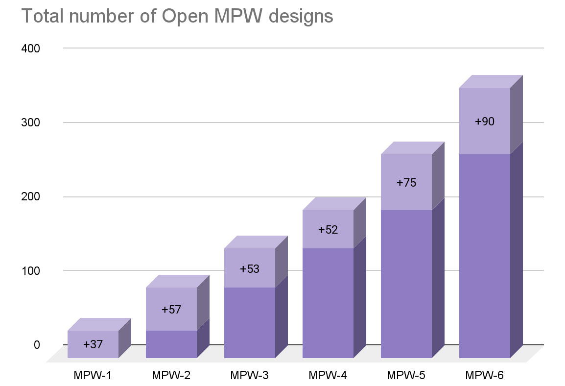
Leading up to the announcement, Google spent two years working with SkyWater Technologies after releasing one of their PDKs under the Apache 2.0 license. Google completed six shuttle runs during this time, filtering through 350 unique chip designs from the community into 240 projects that were manufactured “at no cost.”
Post-pandemic, Google reckons we are moving into a “New Golden Age” of semiconductors, with diverse applications such as mobile, IoT, and automotive all growing strongly. Moreover, its open-source chipmaking venture with GloFo will help give this movement critical momentum.
GloFo is currently the fourth largest chip foundry and manufactures about 6% of the world’s semiconductors. It can output 16+ million wafers at 180nm yearly and plans to increase capacity to 22+ million wafers by 2026.
Google ended its blog post by telling software developers and hardware engineers, researchers and undergrad students, hobbyists and industry veterans, new startups and industry players alike that “we need you.” In some ways, this appeal makes this project look like a gamble by Google, with it betting on the chance that some unknown genius makes something special to kick start the open source silicon ecosystem meaningfully.
Get Tom's Hardware's best news and in-depth reviews, straight to your inbox.

Mark Tyson is a news editor at Tom's Hardware. He enjoys covering the full breadth of PC tech; from business and semiconductor design to products approaching the edge of reason.

