Intel Accidentally Revealed a CPU, Then Pulled it From Public View

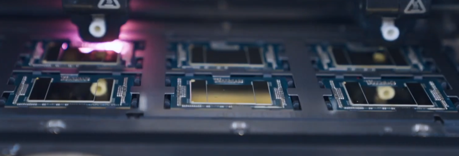
Intel accidentally shared a sneak peek of a next-generation Xeon chip in a promotional video, flaunting the company's advanced packaging technologies. While the chipmaker quickly removed it from the video, we saved a screenshot of the mysterious processor, which poses as a single-die Sierra Forest or Granite Rapids part.
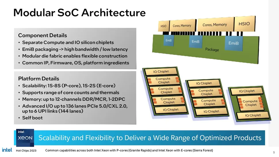
Sierra Forest and Granite Rapids emerged from the shadows at Hot Chips 2023. The processors conform to a tile-based layout, which is an excellent approach toward scalability. The next-generation Xeon chips feature compute chiplets built on the Intel 3 process node and twin I/O chiplets on the older Intel 7 process node. The architectures differ, though. Sierra Forest utilizes Sierra Glen E-cores, whereas Granite Rapids taps into Intel's Redwood Cove P-cores, which power the impending mobile Meteor Lake chips.

According to Intel's diagrams at the Hot Chips 2023 deep dive, Sierra Forest and Granite Rapids could arrive in three different configurations. The first variant consists of three compute chiplets, while the second variant only has two compute chiplets. The third variant is the most interesting since it sports a single-die design. Regardless of the variant, two I/O chiplets will always accompany Sierra Forest and Granite Rapids.


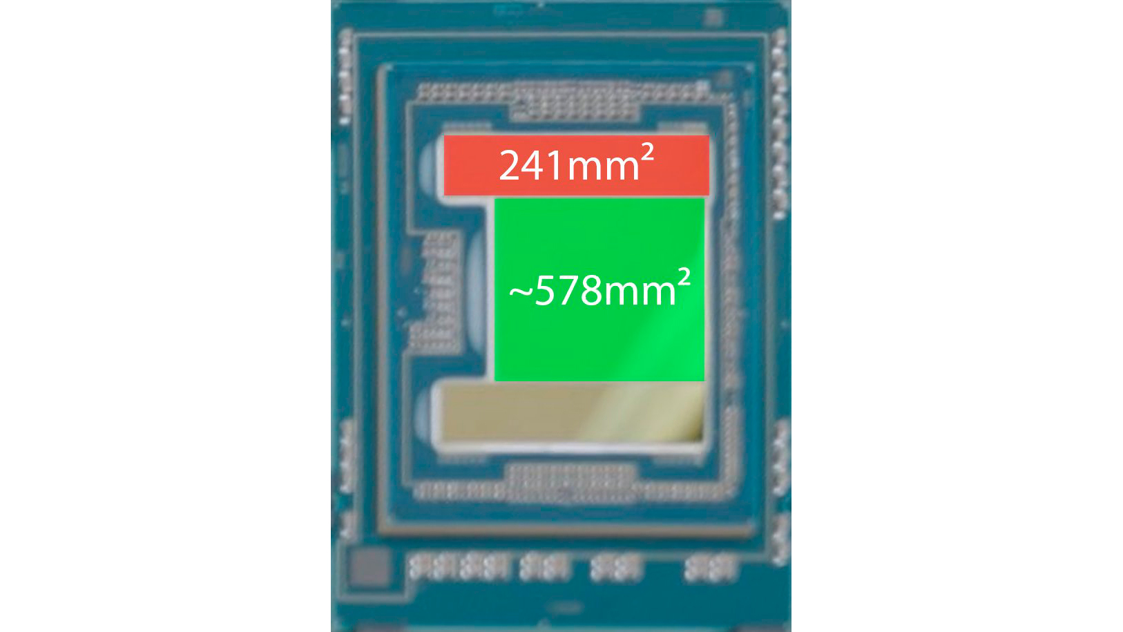
The Xeon processor from Intel's video has a similar design to the single-die variant exhibited at Hot Chips 23. The huge compute chiplet is sandwiched in between the two I/O chiplets. There has been some online chatter speculating the dimensions of the chiplets of the processor. X user Wild_C estimates the compute chiplet to be around 578 mm² and the I/O chiplets to 241 mm², slightly less than half of that of the compute chiplet. Intel hasn't shared the official die sizes for Sierra Forest or Granite Rapids, so treat the approximations with a pinch of salt.
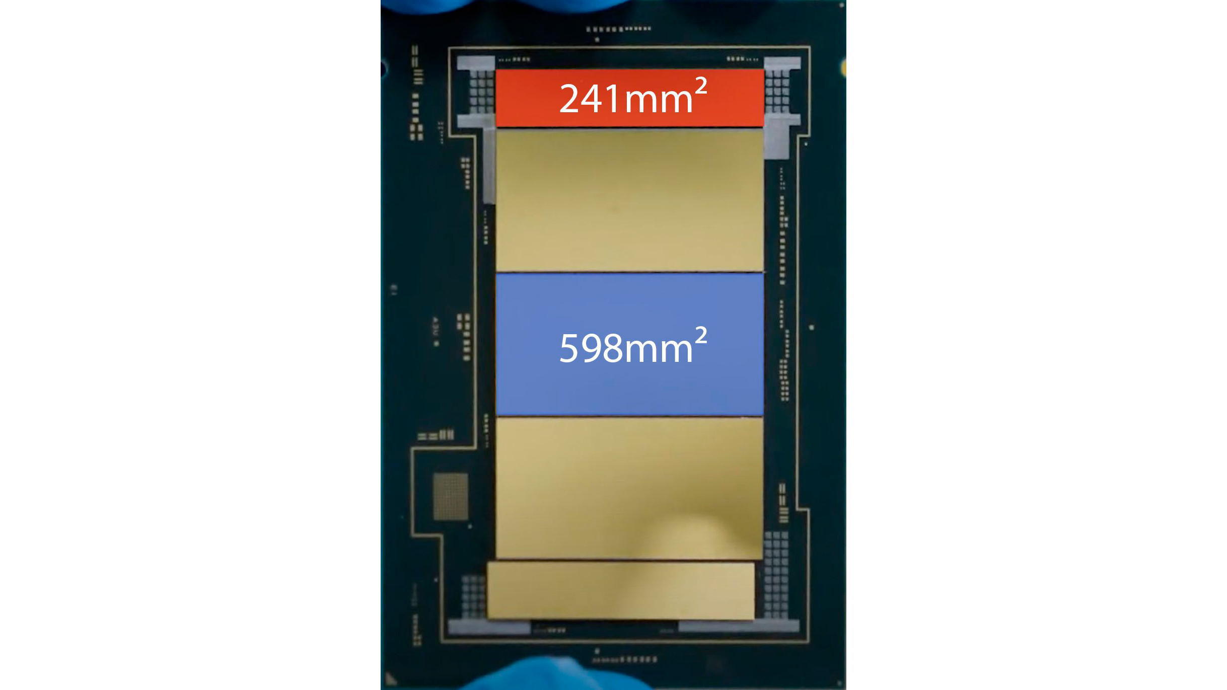
Die Size Measurements for Granite Rapids-AP UCC (left) and Sierra Forest-SP HCC (right):-Birch Stream IO Die (shared): 241mm²-GNR 44P UCC Compute Die: 598mm²-SRF 144E HCC Compute Die: ~578mm² (large margin of error due to low res) pic.twitter.com/ng23f103sMSeptember 8, 2023
If we go with calculated chiplet sizes, the unknown Xeon processor could be Granite Rapids. The current estimation for the compute chiplet in Granite Rapids is approximately 598 mm². The dimensions somewhat align with those of the chip in Intel's video. However, Wild_C admitted that there is a significant margin of error to the estimated measurement due to the low-resolution photograph. Meanwhile, the size of the I/O chiplets seems identical. For all we know, Intel can use the same I/O chiplet for Granite Rapids and Sierra Forest. That's the advantage of disaggregated architectures. Since the memory controller resides on the compute chiplet, it doesn't affect the design.
On the other hand, the Xeon chip could be Sierra Forest. Granite Rapids wields 144 cores over three compute chiplets, equaling 48 P-cores per chiplet. You get around four E-cores in the space of a regular P-core. So that works out to 192 E-cores on a single die, making the scales lean toward Sierra Forest. However, Sierra Forest maxes out at 144 cores, which could explain the smaller compute chiplet compared to a Granite Rapids.
Therefore, it could go either way. But we're more inclined to Sierra Forest, and the math explains it. The problem is that we're uncertain if Intel baked a different chiplet for the single-die Granite Rapids. It's not unheard of because the chipmaker did that with Sapphire Rapids.
Get Tom's Hardware's best news and in-depth reviews, straight to your inbox.

Zhiye Liu is a news editor, memory reviewer, and SSD tester at Tom’s Hardware. Although he loves everything that’s hardware, he has a soft spot for CPUs, GPUs, and RAM.
-
derekullo Silly Intel!Reply
With those pictures alone I will start up my own Fab and start mass producing my own chips!
This will be their greatest blunder!
... besides 14nm++++ -
JayNor "For all we know, Intel can use the same I/O chiplet for Granite Rapids and Sierra Forest."Reply
Intel has stated that Granite Rapids and Sierra Forest shared the same platform, although they also have said that Sierra Forest would not support above 2S configurations ... which implies there could be some restriction on the number of HSIO lanes used for UPI. -
dalek1234 578 mm²? That's a bit on the FAT side. What am I missing here? I thought the purpose of chiplets was to produce smaller dies to keep the cost down due to better yields?Reply -
jp7189 Reply
..or to pack a single package with more silicon than the reticle size limit would normally allow.dalek1234 said:578 mm²? That's a bit on the FAT side. What am I missing here? I thought the purpose of chiplets was to produce smaller dies to keep the cost down due to better yields? -
kjfatl Reply
It is apparent that this die has many identical cores. Each time a chiplet is halved in size the usable area drops by about 20%. The alternative it to include redundant cores that are unused if they fail test. Even if 20% of the cores have failed, Intel will have a saleable part.dalek1234 said:578 mm²? That's a bit on the FAT side. What am I missing here? I thought the purpose of chiplets was to produce smaller dies to keep the cost down due to better yields?