Intel And Micron Announce Shipments Of 3D NAND - Op-Ed
Intel and Micron hosted a joint webcast yesterday titled "Intel and Micron - A Strong Partnership" to announce availability of their 3D NAND technology. On the surface, this seems to be a typical product announcement. However, for those who follow far too many stock and industry analyst RSS feeds, as I am wont to do, the announcement is a clear response to public speculation of a seemingly tense undercurrent between the two companies.
The technological achievements of 3D NAND are astounding, but the larger story is just as interesting. Both Micron and Intel had a representative from each company at two separate locations. One location was in Boise, Idaho, the home of Micron, and the other two representatives were in Intel's bastion in Santa Clara, California. The event was a clear show of solidarity between the two companies, and it was clearly meant to quell the rampant speculation among analysts and industry watchers that has spawned a rash of articles on the topic.
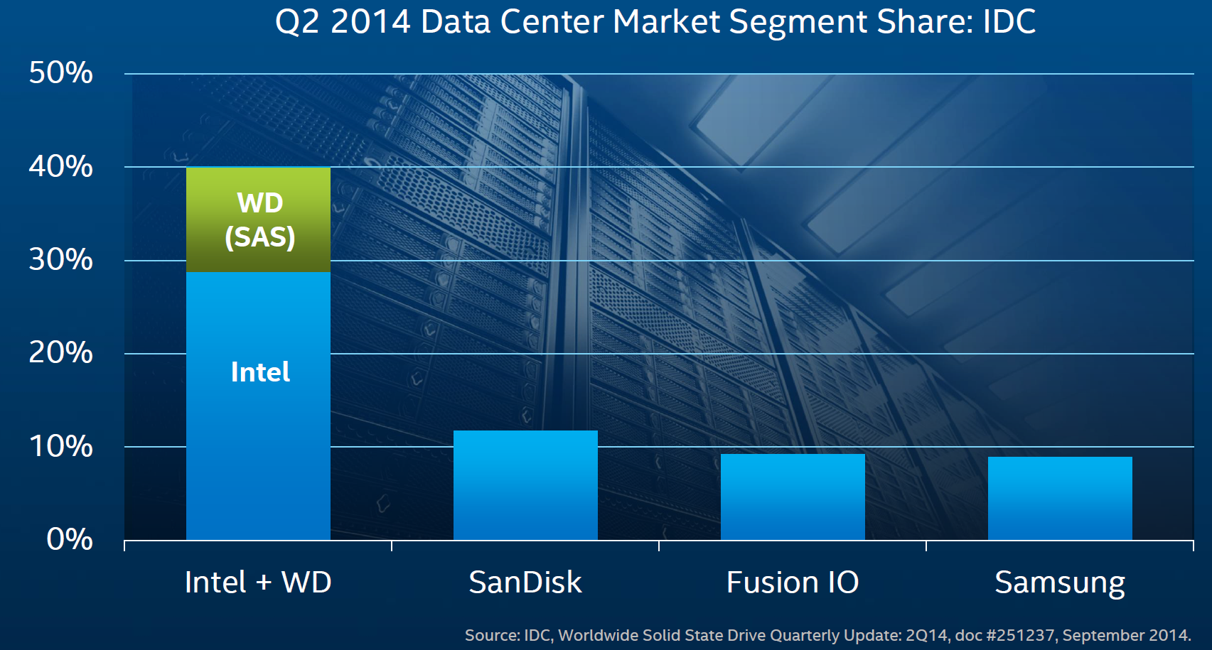
We are going to start at the beginning with a look at this slide from the Intel Investor Meeting in November of last year. This Intel-only event was the original 3D NAND announcement, and here we can see that Intel was flaunting its massive market lead in data center flash products. Micron, one of the other market leaders, was conspicuously absent. Intel likely omitted Micron to avoid posturing itself as superior to its key partner, but Micron's omission highlights the dynamics of the 'frenemy' relationship the two companies share.
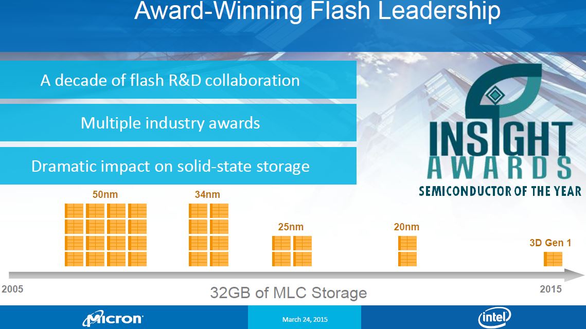
Article continues belowIntel and Micron work together in the IMFT (Intel - Micron Flash Technologies) partnership, and the companies have helped reshape the dynamics of the NAND market over the last decade. What began in 2005 as a simple mission to sell NAND to third-party customers has evolved into a refined marketplace where the NAND fabs aim to produce their own products.
Producing end products, such as SSDs, and enterprise SSDs in particular, delivers a much higher profit margin than merely selling mass quantities of NAND for others to assemble into SSDs, and sell as their own product. In fact, the percentage of NAND that Intel and Micron sell to the open market is declining as they continue to ramp production of their own devices.
In the end, it isn't wise to fuel one's own competition. However, Intel and Micron are doing just that as an unavoidable side effect of the IMFT partnership. The companies are jointly producing NAND, yet competing with each other's finished products.
The real issue at the Intel Investor Meeting involved 3D NAND messaging. Intel, in its exuberance, began referring to the product as having a 'disruptive' cost. Over the following months, Micron's leadership responded with more measured cost expectations that didn't match Intel's message, and this set off another round of speculation in analyst circles. IMFT 3D NAND is the same product for both Intel and Micron, and analysts want to know which version of the timeline, and cost/efficiency expectations, are correct.
Get Tom's Hardware's best news and in-depth reviews, straight to your inbox.
Intel Goes It Alone?
During the Q&A session at last year's Investor Meeting, Intel famously announced that it could produce 3D NAND at its own fabs if it chose to do so. This announcement made many an analyst's ears perk up; Intel producing its own NAND would be a radical departure from the established norms of the IMFT relationship. In a world of scripted events and heavily over-scrutinized comments, very few things are accidentally mentioned or proclaimed. The Intel declaration came off as either a sign of bravado or independence, but some felt it might be an ominous portent of tension in IMFT land.
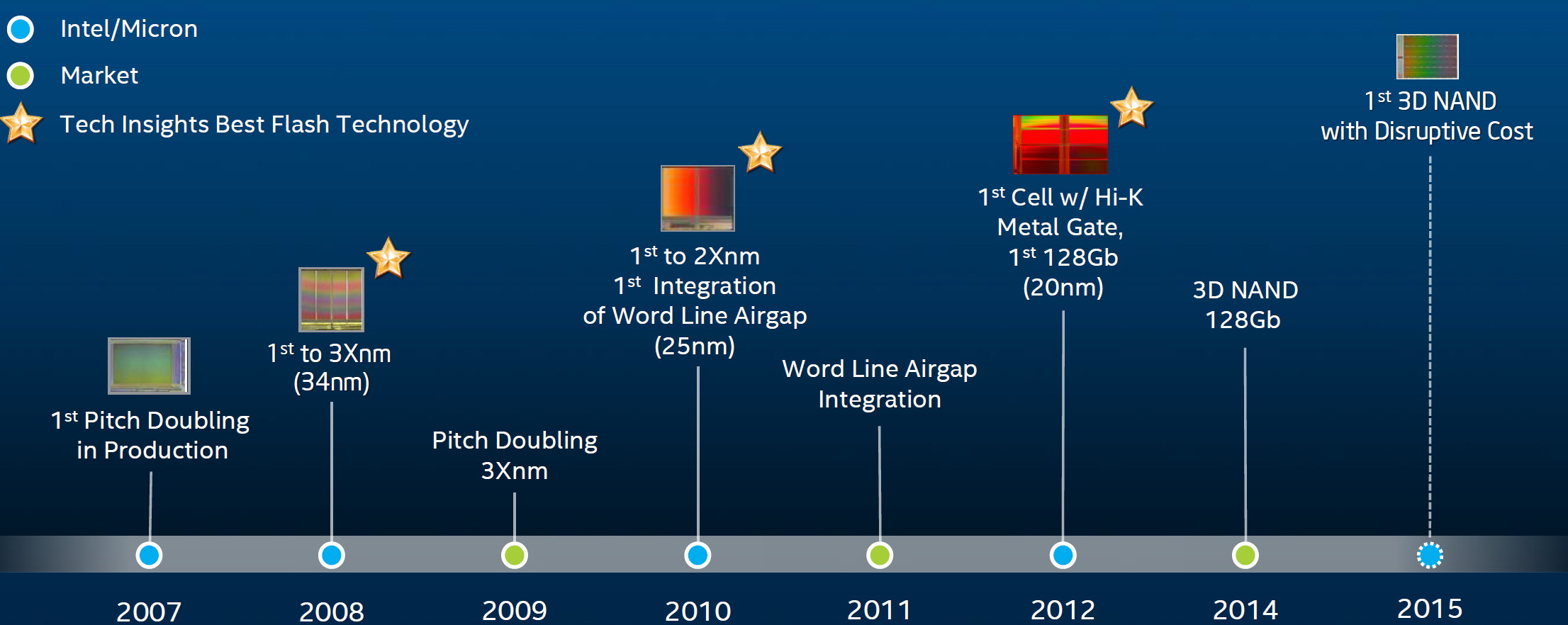
This chart was displayed in yesterday's presentation to illustrate the progress of the IMFT collaboration over the last decade. In reality, this chart likely explains the real source of the mixed messaging. The progression of IMFT tech over the last decade is listed in detail, but 16 nm NAND is missing because Intel chose to forgo investments in 16 nm manufacturing, instead jumping from 20 nm to 3D NAND. There can be several motivations for this jump, including a reluctance to invest in 16 nm equipment that can not be used for future 3D NAND manufacturing.
Intel's strategic move illustrates its incredible confidence in 3D NAND, but leaves Micron as the sole owner of 16 nm manufacturing. It also places tremendous importance on the 3D production timelines moving along within expectations.
Micron is very proud of its 16 nm NAND product, and rightfully so; it has spent tremendous time and treasure on the product over the last several years. During the presentation, Intel announced that 3D NAND is already cost-competitive with IMFT NAND. This is true; 3D NAND is likely cost-competitive with IMFT 20 nm. However, it is almost certainly not comparable to the cost and profit margins of Micron's 16 nm. Eventually, 3D NAND will undoubtedly be a more efficient process than 16 nm, but this will take time, and perhaps even a move to the second generation of the product.
The net effect? Intel is left with an aging 20 nm process that could hold up new product development. Any disruption in 3D NAND production schedules, or unfavorable yields, can affect its competitiveness in a fluid market. Intel has a vested interest in 20 nm through IMFT, but apparently there isn't enough allocation to satisfy its requirements. The company has already been forced into sourcing 20 nm SK Hynix NAND for some of its products, which is unquestionably hurting Intel's profit margins. If the transition to 3D NAND goes well, there is nothing to worry about, but one could understand if there is a fair bit of apprehension.
Micron, by comparison, is reaping the fruits of its 16 nm investment. For the time being, 16 nm will generate higher profits than 3D NAND, and Micron has plenty of it, affording the company plenty of breathing room.
Micron is also investing in moving along quickly with 3D NAND, and it is already expanding its Singapore plant by an additional 225,000 square feet to handle the demand. The IMFT facility in Lehi, Utah will also produce 3D NAND. IMFT expects mass production of both MLC and TLC 3D NAND in 2H 2015, and finished products are set to arrive in 2016.
In the background of these developments the world of flash storage is beginning to move at breakneck speed. Samsung continues to expand its lead with 3D V-NAND, and other manufacturers, such as Toshiba, are getting closer to bringing new 3D NAND architectures to the market. We break down the overall progress of the broader 3D NAND market in our Toshiba Unveils 48-Layer BiCS 3D NAND article.
And Now, IMFT 3D NAND
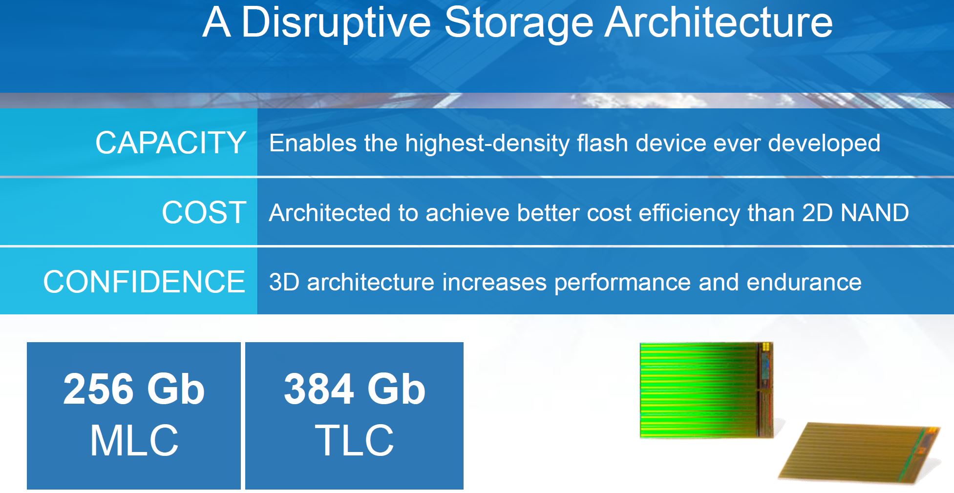
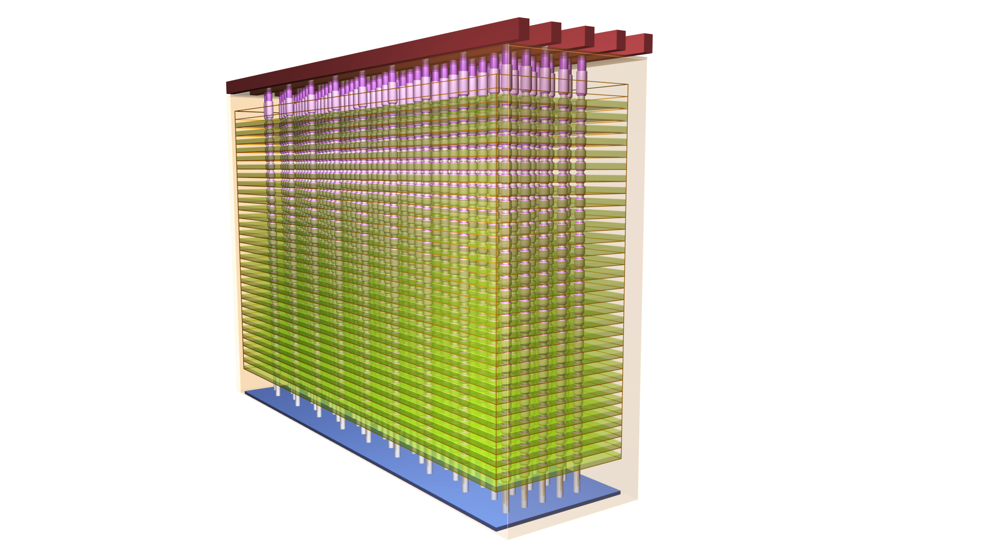
Notice the "disruptive" term in this slide from yesterdays presentation? The IMFT 3D NAND is disruptive, comes with 32 layers and has a die density of 256 Gb (32 GB) for MLC and 384 Gb (48 GB) for TLC. All of IMFT's competitors are either at 128 Gb or 86 Gb dies, so IMFT has taken the lead from a pure die density aspect.
Intel divulged that 16 die can be stacked into a single package. This creates a single 512 GB MLC package, or an astounding 784 GB TLC package, enabling a density revolution in every facet of the storage realm. These small chips will offer incredible density in mobile phones and devices, enabling slim m.2 SSDs with 3.5 TB of capacity, and even creating 10 TB 2.5" SSDs.
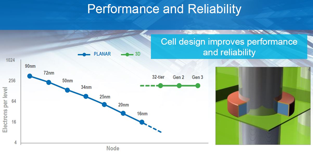
The 3D NAND design addresses the inherent scaling issues with planar (2D) NAND. As each successive generation of planar NAND decreases in size, it loses the ability to hold as many electrons per cell. This has a direct impact on performance and error rates. Eventually, the overhead of dealing with these errors, and the need for more overprovisioning to offset the reduced endurance, creates an untenable situation. 3D NAND relaxes the lithography and allows the electrons-per-cell equivalency of a 50 nm device.
IMFT is leveraging its collective experience with a floating gate design for its 3D NAND, indicating this will enable Moore's Law to take effect for several product generations to come. Other competitors, such as Samsung and Toshiba/SanDisk, are moving to Charge Trap, instead of floating gates. These competing approaches will take a much more in-depth comparison to cover adequately; but suffice it to say, the winner will be dictated by cost efficiency, scalability, endurance and performance. This will be impossible to ascertain, even partially, before end products begin shipping.
In the future, IMFT can either shrink the lithography or add more layers, or both at once, to increase density. Intel will not disclose the 3D NAND lithography, but the chart indicates they expect to maintain the same electrical equivalency with future generations. This might indicate IMFT is taking a relatively easy approach and simply stacking layers higher for future density increases.
We reached out for additional comment and clarification of other reports that indicate a limited endurance rating on initial products. Micron responded that IMFT is not officially releasing specific endurance metrics, but indicated the MLC 3D NAND solutions will meet or exceed the endurance of planar 20 nm NAND.
The new architecture utilizes a 4 plane design, which doubles the number of simultaneously addressable bytes in comparison to the 2 plane design used in its planar NAND. This is crucial for maintaining performance since the number of die/packages in the finished product will inevitably be reduced due to the higher capacity of the die. IMFT also revealed the NAND supports fast 4k read mode, advanced single-pass MLC programming and the ONFI 4 interface. We expect more details to emerge as the products move closer to market.
Any tension in the IMFT camp, be it real or imagined, is likely the result of the two partners trying to navigate an extremely complex but mutually beneficial relationship. Over the past decade, IMFT's technology and products have truly helped revolutionize data storage, and our lives along with it. From the phones in our hands, to the laptops in our laps, and the remote data center that powers it all, NAND touches everyone's lives on a daily basis. Amazingly, this transformative product has only penetrated into four percent of the broader storage market, but IMFT hopes to expand that to seven percent, or more, by 2018. Here's hoping IMFT can reach its unified vision of success in the future.
Follow us @tomshardware, on Facebook and on Google+.

Paul Alcorn is the Editor-in-Chief for Tom's Hardware US. He also writes news and reviews on CPUs, storage, and enterprise hardware.
-
Kewlx25 Glad I didn't build an SSD NAS yet. Prices will keep going down. SSDs came out at the perfect time, just as 3D stacking was coming around.Reply
Next big thing, 4GB+ of L4 3D stacked memory on your CPU. -
Kewlx25 The Nvidia GPUs scheduled for next year will have 4GB-8GB of 3D stacked memory on top of the GPU, directly integrated. 1024bit wide, nearly 1TB/s of bandwidth, half the latency of regular system memory. That's more bandwidth than L1 cache on most CPUs, just not less latency.Reply -
16nm NAND is a bad idea in any case. I don't care how cheap it is, it doesn't last long and is not reliable.Reply
It's cool to see 3d NAND coming from several sources. -
Kewlx25 20nm TLC has 1k write cycles, 20nm 3D has about 10k-35k write cycles depending on the desired performance. 20nm SLC has about 100k cycles.Reply
You can write about 1.5-2.5PB to a 256GB 3D drive before it hits its limit. That's about 8k full drive writes. Once we start seeing 4TB SSDs, even if they drop down to 4k write cycles, you're still talking about 8PB of data written. Plenty for your home user. -
none12345 "The Nvidia GPUs scheduled for next year will have 4GB-8GB of 3D stacked memory on top of the GPU, directly integrated. 1024bit wide, nearly 1TB/s of bandwidth, half the latency of regular system memory. That's more bandwidth than L1 cache on most CPUs, just not less latency. "Reply
The AMD gpus due out very soon, will be the first to have stacked memory on the cpu. We wont have to wait for next year. We will know what kinda performance it brings soon. Dont know when the 3xx series is due. Maybe a month or 2, but not long. -
dstarr3 Honestly, this is the most exciting new technology I've seen coming in a long time. I can't wait to see how this revolutionizes computing.Reply -
Lovolt ReplyFirst paragraph - "as I am wont to do" WUT?
Perhaps the author majored in English and not texting.
