Micron Takes Lead With 232-Layer NAND Flash, up to 2TB per Chip Package
Stackin' them bits.
Micron announced today that it is shipping 232-Layer TLC NAND, taking the lead in the industry with the highest layer count. The new NAND flash comes with the highest density in the industry, enabling up to 2 TB of storage in a single NAND chip package. Micron pairs the improved capacity with up to 100% faster write speeds and more than 75% faster read performance per die over the previous gen, marking a leap forward on the performance front, too. Micron is already shipping this flash in unspecified retail Crucial SSDs, and as NAND components to other manufacturers.
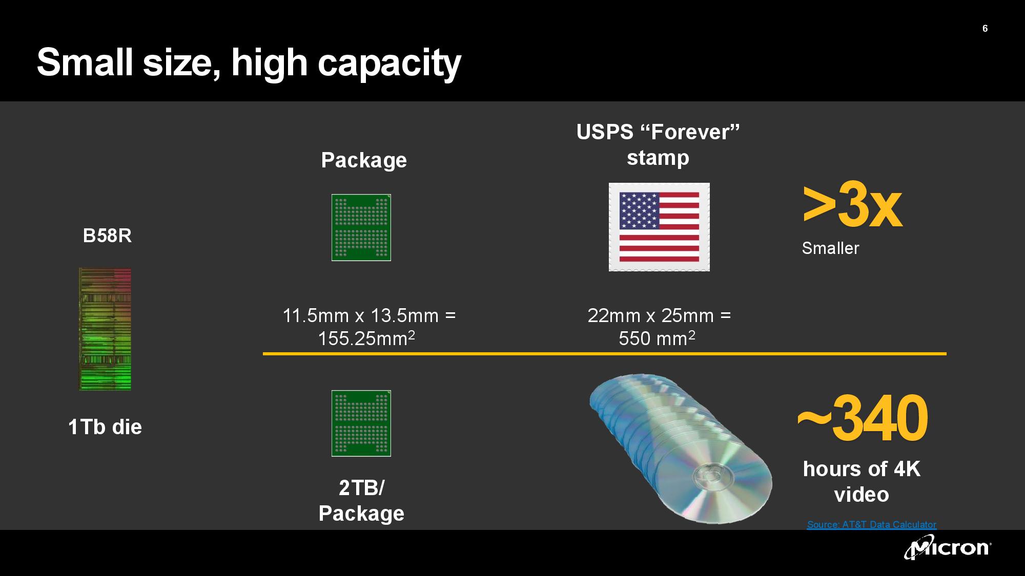
As you can see in the slide below, the increased storage density allowed Micron to shrink the overall package by 28% over its prior-gen flash, which will come in handy for smaller devices like smartphones and MicroSD cards. Each 2TB chip package is three times smaller than a US postage stamp, measuring an incredible 11.5 x 13.5mm. Micron notes you can store 340 hours of 4K video in a single 2TB chip package.
| Row 0 - Cell 0 | Micron | Samsung | WD/Kioxia | SK hynix | YMTC |
| Shipping Now | 232-Layer | 128-Layer | 162-Layer | 176-Layer | 128-Layer |
| Density per square mm | 14.6 Gb mm^2 | 6.91 Gb mm^2 | 10.4 Gb mm^2 | 10.8 Gb mm^2 | 8.48 Gb mm^2 |
| Die Capacity | 1 Tb | 512 Gb | 1 Tb | 512 Gb | 512 Gb |
| Next-Gen (release date) | ? | 3xx (unknown) | 212 (unknown) | 238-Layer (2023) | 196-Layer (2H, 2022) |
Micron's 232 Layer (232L) is a nice step up from the company's previous-gen 176L flash, but it also outstrips the competition in layer counts. However, density is the more important metric. Micron's TLC flash, lovingly named B58R, packs 1Tb of storage into a single small die. Sixteen dies can fit into a package, enabling up to 2TB in a single chip package.
The flash density works out to 14.6 Gb of storage per mm^2, which Micron claims is a lead of between 30% to 100% over competing TLC flash that's currently shipping (we're following up for clarity on that claim). That means each of Micron's dies should be roughly 69mm^2. As before, Micron uses its CMOS under the Array (CuA) tech, now in its sixth generation, to enhance the density by stacking the CMOS under the data storage array. Micron also uses a dual-stack flash design, meaning each finished die is comprised of two 116-Layer dies bonded together in a process called string stacking. Micron also cites advanced processes for creating high-aspect ratio holes and materials advances as contributors to the increased density.
We'll see even higher density when Micron starts producing its QLC variant, but the company isn't sharing the details yet.
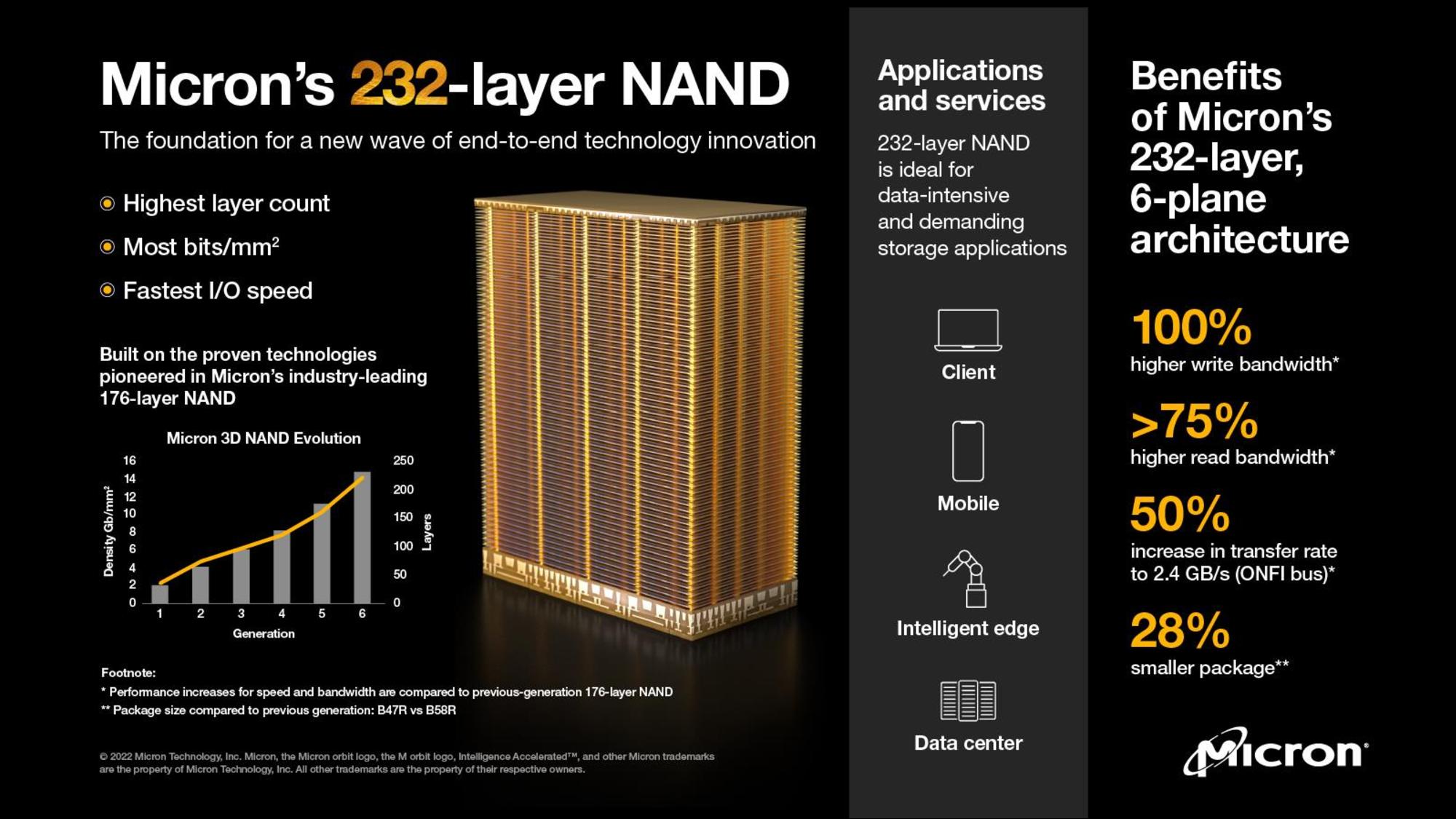
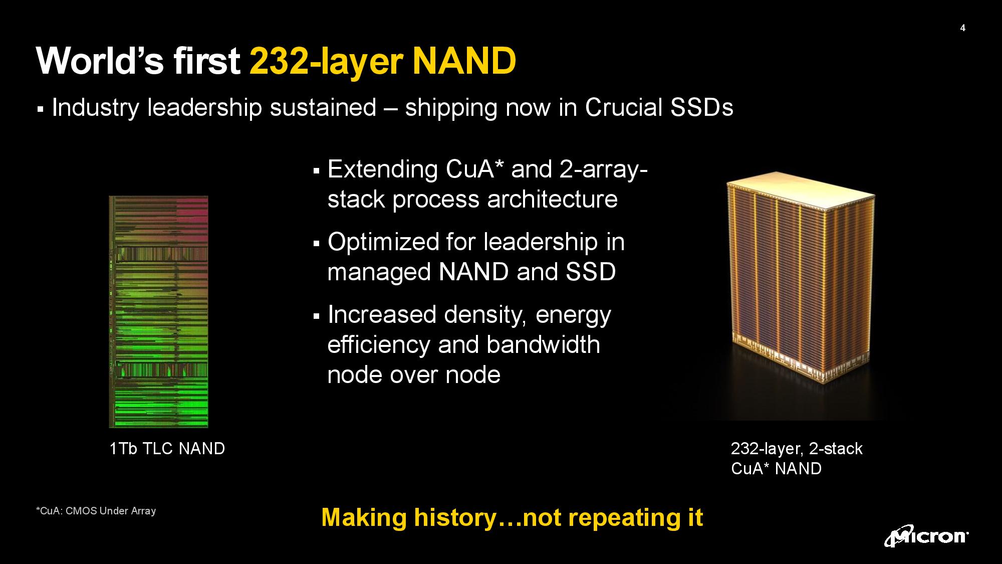
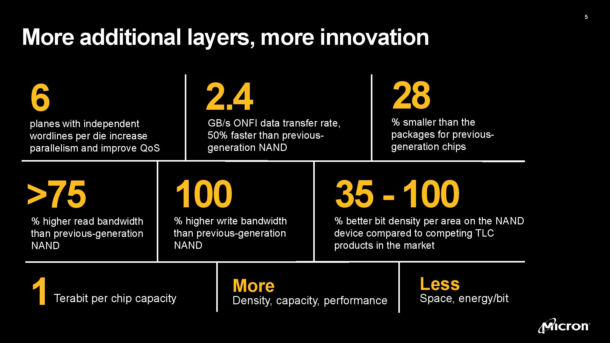

Micron touts impressive performance improvements, too, due to its new six-plane architecture — an industry first for shipping TLC NAND. A plane is a region of a flash die that can respond to I/O requests independently, much like cores in a CPU can each complete operations in parallel. If designed correctly, more planes equate to more performance.
Micron's move from four to six planes, coupled with its 50% increase to 2.4 GB/s over the ONFI 5.0 interface to provide more bandwidth from the die, contributes to what Micron claims is 100% higher write bandwidth and more than 75% higher read bandwidth than its previous-gen 176-Layer NAND. Naturally, that doesn't mean we'll see SSDs that are suddenly twice as fast as existing drives — other bottlenecks still exist, like the controller and interface — but it does pave the way for much faster devices as the rest of the ecosystem catches up to the speed of the new flash.
Micron says the additional planes also confer quality of service and read/write latency improvements due to fewer I/O 'collisions' on the internal pathways, but the company isn't sharing read and write latency metrics yet. The 232L flash now supports a low-voltage NV-LPPDR4 interface that reduces per-bit energy use by 30% over prior-gen interfaces. Micron claims generational energy efficiency gains but hasn't shared firm metrics yet. We're told we'll learn more in the future.
Micron isn't sharing endurance metrics, either, but it expects its 232L TLC to generally match the same endurance thresholds as its previous-gen flash. As a reminder, endurance is rated in Program/Erase (P/E) cycles. For perspective, Micron's previous-gen TLC typically fell within the 1,000 to 3,000 P/E cycle range for consumer SSDs, and 5,000 to 10,000 cycles for enterprise SSDs. Naturally, that's impacted by the type of error correcting code (ECC) employed, but we can expect a similar range for 232L TLC.
Micron's 232L TLC flash is already shipping to its OEM customers as NAND dies and in unspecified retail-facing Crucial SSDs. Micron is still in the early stages of its production ramp but says it will ramp volume throughout 2022. We'll see other versions of this tech, like the QLC variant, emerge in the near future, too.
Get Tom's Hardware's best news and in-depth reviews, straight to your inbox.

Paul Alcorn is the Editor-in-Chief for Tom's Hardware US. He also writes news and reviews on CPUs, storage, and enterprise hardware.
-
peachpuff 100 layer, 200 layer yet 1tb is still $100 😵💫Reply
Only thing being stacked is their profits. -
Kamen Rider Blade Reply
You honestly didn't expect newer, more dense NAND Flash tech to be "Cheaper" then previous generations right away, did you?peachpuff said:100 layer, 200 layer yet 1tb is still $100 😵💫
Only thing being stacked is their profits.
They got to pay off tooling, fab, and R&D costs. -
peachpuff Reply
Using that logic the layers will keep going up while the prices will stay the same? That doesn't compute.Kamen Rider Blade said:You honestly didn't expect newer, more dense NAND Flash tech to be "Cheaper" then previous generations right away, did you?
They got to pay off tooling, fab, and R&D costs. -
Kamen Rider Blade Reply
Do you know how the NAND Flash makers behave?peachpuff said:Using that logic the layers will keep going up while the prices will stay the same? That doesn't compute.
Those memory manufacturers have been caught colluding and price fixing on MULTIPLE occaisions.
Go back and look at Tech History.