MycelioTronics Wants to Create PCBs From Fungi
A recipe for future electronics

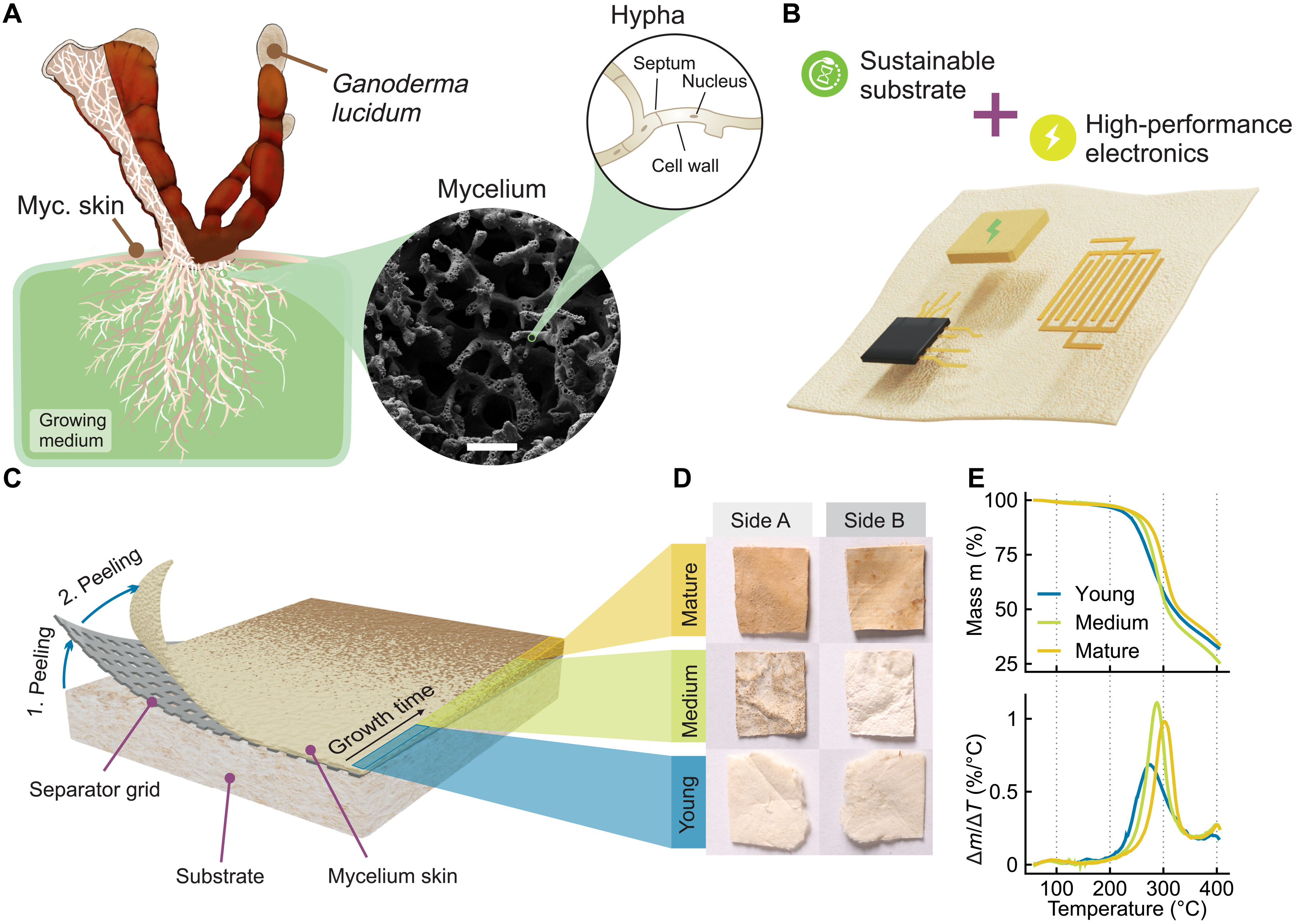
Australian company MycelioTronics is trying to solve the electronics waste problem by tackling it in a creative, biomaterials approach that replaces the usual layering components in a PCB with fungal mycelium skin. This mycelium skin, extracted from the mushroom Ganoderma lucidum's, has been shown to develop PCB-like qualities (such as thermal resistance, flexibility, and insulation) while also allowing for much easier decomposition and recycling processes due to its biological origin.
The electronics industry has mixed sustainability practices. This is especially true in PCBs, which make use of rare minerals (such as copper and gold), epoxy resins, and chemical elements so intricately connected, wired and sandwiched together that recycling efforts are extremely difficult. Recycling usually leads to the use of environmentally-damaging chemicals that allow for the separation of some of its component materials.
Dr. Martin Kaltenbrunner states "Electronic devices are irrevocably integrated into our lives," the researchers explained. "Yet, their limited lifetime and often improvident disposal demands sustainable concepts to realize a green electronic future. Research must shift its focus on substituting nondegradable and difficult-to-recycle materials to allow either biodegradation or facile recycling of electronic devices."
Of course, there's also the matter of planned obsolescence and manufacturing practices that make these processes even more difficult. In turn, these have generated movements such as Right to Repair and even forced Apple's adoption of the USB standard on its future iPhones (the less cable types there are, the lesser number of them will become obsolete). One of the ways companies and researchers are looking into reducing the electronics industry's overall footprint is by finding biomaterial alternatives that reduce this environmental cost whilst not hindering the pace of technological innovation.

According to the researchers, the mycelium skin present in Ganoderma lucidum's is one such material: it's both thin and flexible while maintaining a strong structural integrity. It's been able to withstand around 2000 bending cycles; it shows only moderate resistance when folded; it insulates electrical currents; and can sustain temperatures that reach 250 degrees Celsius, which is higher than even top PCB assemblies (which are usually rated up to 150 degrees Celsius). This heat resistance makes the mycelium skin an attractive proposition for actually implanting components (such as CPUs and others) through traditional soldering; and interestingly, the older the mycelium skin, the higher its thermal ceiling.
So all the hallmarks for a PCB replacement are there - with the added bonus that mycelium-based PCBs such as these could be made to biodegrade whenever their shelf life is over. It only needs water (something you wouldn't want in your non-obsolete electronics anyway) or UV lighting. Absent of these two elements, the scientists say, the mycelium-based PCB could last for hundreds of years.
Of course, the mycelium skin doesn't function as a PCB all by itself; its properties are those of an insulator, which means conducting capabilities must be added to it in order to create a biomaterial PCB. So the researchers applied coatings of copper, chromium, and even gold (a process known as physical vapor deposition [PVD]) to the mycelium skin that added the required electric conductivity properties. The newly-formed material was then ablated with lasers (much like typical PCBs are) to remove the excess minerals, leaving behind the conductive lanes that carry electrical signals throughout.
Get Tom's Hardware's best news and in-depth reviews, straight to your inbox.
Mycelium networks (also known as a mycorrhizal networks) are some of the most interesting structures in the natural world, and allow for a veritable network of fungi, plants and trees to "communicate" through the transfer of water, nitrogen, carbon and other minerals. Through this network, trees can share their resources with one another in what amounts to a decentralized system of feedback loops. You may be surpised to know that this network covers most of the world's landmass.

Francisco Pires is a freelance news writer for Tom's Hardware with a soft side for quantum computing.
-
Pretty interesting discovery and finding. Thanks for the article. It really makes one wonder as to how far Science/tech and research has advanced and progressed these days, compared to yore.Reply
-
Samo Paulini For me as a biologist it would be helpful to mention that you mean printed circuit boards and not polychlorinated biphenyls somewhere in the article.Reply -
The User Reply
Already the first word is wrong....Admin said:Australia-based MycelioTronics is looking for a way to reduce electronic waste by converting the tried and true PCB (Printed Circuit Board) towards a more environmentally friendly - and perhaps surprisingly adequate - mycellium-based solution.
MycelioTronics Wants to Create PCBs From Fungi : Read more
AUSTRIAN, not Australian.